- 您現(xiàn)在的位置:買賣IC網(wǎng) > PDF目錄370458 > HD4043612 (Hitachi,Ltd.) 4-bit HMCS400-Series microcomputer(4位單片微計(jì)算機(jī)) PDF資料下載
參數(shù)資料
| 型號: | HD4043612 |
| 廠商: | Hitachi,Ltd. |
| 英文描述: | 4-bit HMCS400-Series microcomputer(4位單片微計(jì)算機(jī)) |
| 中文描述: | 4位HMCS400系列微機(jī)(4位單片微計(jì)算機(jī)) |
| 文件頁數(shù): | 8/115頁 |
| 文件大小: | 710K |
| 代理商: | HD4043612 |
第1頁第2頁第3頁第4頁第5頁第6頁第7頁當(dāng)前第8頁第9頁第10頁第11頁第12頁第13頁第14頁第15頁第16頁第17頁第18頁第19頁第20頁第21頁第22頁第23頁第24頁第25頁第26頁第27頁第28頁第29頁第30頁第31頁第32頁第33頁第34頁第35頁第36頁第37頁第38頁第39頁第40頁第41頁第42頁第43頁第44頁第45頁第46頁第47頁第48頁第49頁第50頁第51頁第52頁第53頁第54頁第55頁第56頁第57頁第58頁第59頁第60頁第61頁第62頁第63頁第64頁第65頁第66頁第67頁第68頁第69頁第70頁第71頁第72頁第73頁第74頁第75頁第76頁第77頁第78頁第79頁第80頁第81頁第82頁第83頁第84頁第85頁第86頁第87頁第88頁第89頁第90頁第91頁第92頁第93頁第94頁第95頁第96頁第97頁第98頁第99頁第100頁第101頁第102頁第103頁第104頁第105頁第106頁第107頁第108頁第109頁第110頁第111頁第112頁第113頁第114頁第115頁
HD404369 Series
8
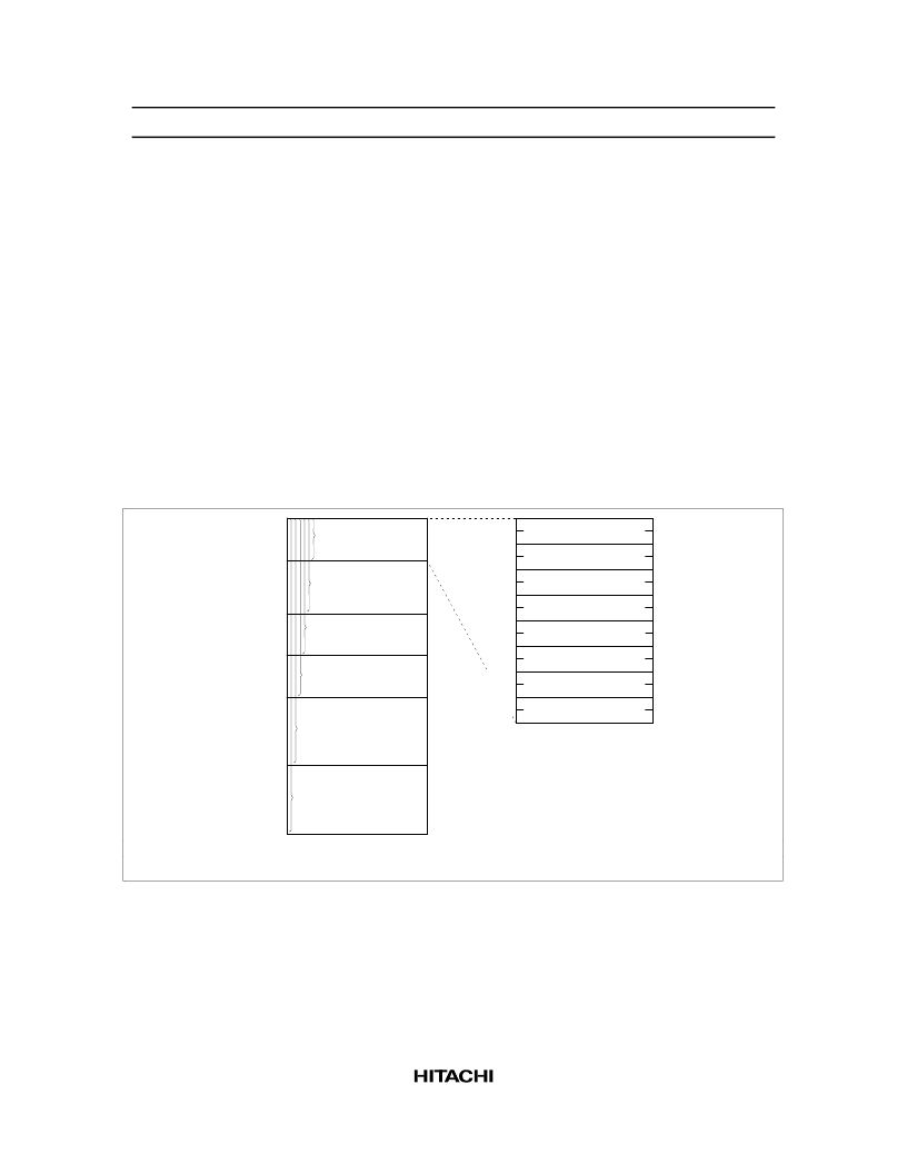
Memory Map
ROM Memory Map
The ROM memory map is shown in figure 1 and described below.
Vector Address Area ($0000–$000F):
Reserved for JMPL instructions that branch to the start addresses
of the reset and interrupt routines. After MCU reset or an interrupt, program execution continues from the
vector address.
Zero-Page Subroutine Area ($0000–$003F):
Reserved for subroutines. The program branches to a
subroutine in this area in response to the CAL instruction.
Pattern Area ($0000–$0FFF):
Contains ROM data that can be referenced with the P instruction.
Program Area ($0000-$0FFF (HD404364, HD40A4364), $0000–$1FFF (HD404368, HD40A4368),
$0000–$2FFF (HD4043612, HD40A43612), $0000–$3FFF (HD404369, HD40A4369, HD407A4369)):
The entire ROM area can be used for program coding.
$000F
$0010
$0FFF
$1000
$2FFF
$003F
$0040
Vector address
(16 words)
Zero-page subroutine
(64 words)
Program
(4,096 words)
For HD404364, HD40A4364
Program
(8,192 words)
For HD404368, HD40A4368
$0000
$0000
$0001
$0002
$0003
$0004
$0005
$0006
$0007
$0008
$0009
$000A
$000B
$000C
$000D
$000E
$000F
JMPL instruction
(jump to
RESET
,
STOPC
routine)
JMPL instruction
(jump to
INT
routine)
JMPL instruction
(jump to timer A routine)
JMPL instruction
(jump to timer B routine)
JMPL instruction
(jump to timer C routine)
JMPL instruction
(jump to A/D converter routine)
JMPL instruction
(jump to
INT
routine)
JMPL instruction
(jump to serial routine)
Program
(12,288 words)
Program
(16,384 words)
For HD404369, HD40A4369,
HD407A4369
$1FFF
$2000
$3000
$3FFF
For HD4043612, HD40A43612
Note:
Since the ROM address areas between $0000–$0FFF overlap, the user can determine how these
areas are to be used.
Figure 1 ROM Memory Map
RAM Memory Map
The MCU contains 512-digit
×
4 bit RAM areas. These RAM areas consist of a memory register area, a
data area, and a stack area. In addition, an interrupt control bits area, special function register area, and
register flag area are mapped onto the same RAM memory space labeled as a RAM-mapped register area.
The RAM memory map is shown in figure 2 and described below.
相關(guān)PDF資料 |
PDF描述 |
|---|---|
| HD404369 | 4-bit HMCS400-Series microcomputer |
| HD404369H | 4-bit HMCS400-Series microcomputer |
| HD404369S | 4-bit HMCS400-Series microcomputer |
| HD404369F | 4-bit HMCS400-Series microcomputer |
| HD404372 | Low-Voltage AS Microcomputers with On-Chip A/D Converter(帶片上A/D轉(zhuǎn)換器的低壓微計(jì)算機(jī)) |
相關(guān)代理商/技術(shù)參數(shù) |
參數(shù)描述 |
|---|---|
| HD4043612F | 制造商:HITACHI 制造商全稱:Hitachi Semiconductor 功能描述:4-bit HMCS400-Series microcomputer |
| HD4043612H | 制造商:RENESAS 制造商全稱:Renesas Technology Corp 功能描述:microcomputer has an A/D converter |
| HD4043612S | 制造商:HITACHI 制造商全稱:Hitachi Semiconductor 功能描述:4-bit HMCS400-Series microcomputer |
| HD404364 | 制造商:未知廠家 制造商全稱:未知廠家 功能描述:HMCS43XXFamily User's Manual/Device |
| HD404364F | 制造商:RENESAS 制造商全稱:Renesas Technology Corp 功能描述:microcomputer has an A/D converter |
發(fā)布緊急采購,3分鐘左右您將得到回復(fù)。