- 您現(xiàn)在的位置:買賣IC網(wǎng) > PDF目錄385354 > HC5504B (Intersil Corporation) EIA/ITU PABX SLIC with 40mA Loop Feed PDF資料下載
參數(shù)資料
| 型號: | HC5504B |
| 廠商: | Intersil Corporation |
| 英文描述: | EIA/ITU PABX SLIC with 40mA Loop Feed |
| 中文描述: | 環(huán)境影響評估/國際電聯(lián)交換機用戶接口與四十○毫安環(huán)飼料 |
| 文件頁數(shù): | 6/9頁 |
| 文件大?。?/td> | 224K |
| 代理商: | HC5504B |
6
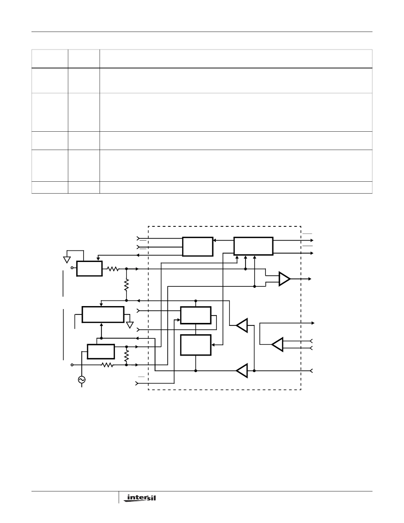
Functional Diagram
21
RX
Receive Input, 4-Wire Side - A high impedance analog input which is internally biased. Capacitive coupling to this
input is required. AC signals appearing at this input differentially drive the Tip feed and Ring feed terminals, which in
turn drive tip and ring through 300
of feed resistance on each side of the line.
22
C
4
Capacitor #4 - An external capacitor to be connected between this terminal and analog ground. This capacitor
prevents false ground key indication and false ring trip detection from occurring when longitudinal currents are
induced onto the subscriber loop from near by power lines and other noise sources. This capacitor is also required
for the proper operation of ring trip detection. Typical value is 0.5
μ
F, to 1.0
μ
F, 20V. This capacitor should be
nonpolarized.
23
AG
(Note 5)
Analog Ground - To be connected to zero potential and serves as a reference for the transmit output (TX) and receive
input (RX) terminals.
24
TX
Transmit Output, 4-Wire Side - A low impedance analog output which represents the differential voltage across Tip
and Ring. Transhybrid balancing must be performed (using the SLIC microcircuit’s spare op amp) beyond this output
to completely implement two to four wire conversion. This output is unbalanced and referenced to analog ground.
Since the DC level of this output varies with loop current, capacitive coupling to the next stage is essential.
NC
No internal connection.
Pin Descriptions
(Continued)
24 PIN
SOIC
SYMBOL
DESCRIPTION
LOOP
MONITORING
RING
CONTROL
2 WIRE
LOOP
SECONDARY
PROTECTION
LINE
DRIVERS
TIP
RING
V
B
-
V
B
-
PD
POWER DENIAL
150
RING
150
RF
BG
150
TF
TIP
RD
RC
RS
RING SYNC
RING COMMAND
RING
TRIP
SHD
GKD
OUT
RX
RECEIVE
INPUT
SLIC MICROCIRCUIT
1/2 RING
RELAY
V
B
-
RING
VOLTAGE
RFS
1/2 RING
RELAY
150
SWITCH HOOK
DETECTION
GROUND KEY
DETECTION
BATTERY
FEED
LOOP
CURRENT
LIMITER
DIFF
AMP
TX
TRANSMIT
OUTPUT
+
-
+1
-1
OP
AMP
+IN
-IN
+
-
HC-5504B
相關PDF資料 |
PDF描述 |
|---|---|
| HC5509A1R3060 | SLIC Subscriber Line Interface Circuit |
| HC4P5509A1R3060 | SLIC Subscriber Line Interface Circuit |
| HC5521 | SLIC Subscriber Line Interface Circuit |
| HC5521CM | SLIC Subscriber Line Interface Circuit |
| HC5521CQ | SLIC Subscriber Line Interface Circuit |
相關代理商/技術參數(shù) |
參數(shù)描述 |
|---|---|
| HC-5504B | 制造商:INTERSIL 制造商全稱:Intersil Corporation 功能描述:EIA/ITU PABX SLIC with 40mA Loop Feed |
| HC-5504B_04 | 制造商:INTERSIL 制造商全稱:Intersil Corporation 功能描述:EIA/ITU PABX SLIC with 40mA Loop Feed |
| HC-5504B1 | 制造商:INTERSIL 制造商全稱:Intersil Corporation 功能描述:ITU Low Cost, PABX SLIC With 40mA Loop Feed |
| HC-5504B1_03 | 制造商:INTERSIL 制造商全稱:Intersil Corporation 功能描述:ITU Low Cost, PABX SLIC With 40mA Loop Feed |
| HC5504B3 | 制造商:未知廠家 制造商全稱:未知廠家 功能描述:Telecommunication IC |
發(fā)布緊急采購,3分鐘左右您將得到回復。