- 您現(xiàn)在的位置:買賣IC網(wǎng) > PDF目錄370390 > GS88136T-80I x36 Fast Synchronous SRAM PDF資料下載
參數(shù)資料
| 型號(hào): | GS88136T-80I |
| 英文描述: | x36 Fast Synchronous SRAM |
| 中文描述: | x36快速同步SRAM |
| 文件頁(yè)數(shù): | 24/33頁(yè) |
| 文件大?。?/td> | 616K |
| 代理商: | GS88136T-80I |
第1頁(yè)第2頁(yè)第3頁(yè)第4頁(yè)第5頁(yè)第6頁(yè)第7頁(yè)第8頁(yè)第9頁(yè)第10頁(yè)第11頁(yè)第12頁(yè)第13頁(yè)第14頁(yè)第15頁(yè)第16頁(yè)第17頁(yè)第18頁(yè)第19頁(yè)第20頁(yè)第21頁(yè)第22頁(yè)第23頁(yè)當(dāng)前第24頁(yè)第25頁(yè)第26頁(yè)第27頁(yè)第28頁(yè)第29頁(yè)第30頁(yè)第31頁(yè)第32頁(yè)第33頁(yè)
Rev: 1.10 7/2000
Specifications cited are subject to change without notice. For latest documentation see http://www.gsitechnology.com
24/33
2000, Giga Semconductor, Inc.
Preliminary
GS88118/36T-11/11.5/100/80/66
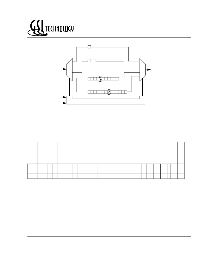
JTAG TAP Block Diagram
Identification (ID) Register
The ID Register is a 32-bit register that is loaded with a device and vendor specific 32-bit code when the controller is put in Capture-DR state with
the IDCODE command loaded in the Instruction Register. The code is loaded froma 32-bit on-chip ROM. It describes various attributes of the
RAMas indicated below. The register is then placed between the TDI and TDO pins when the controller is moved into Shift-DR state. Bit 0 in the
register is the LSB and the first to reach TDO when shifting begins.
ID Register Contents
Tap Controller Instruction Set
Overview
There are two classes of instructions defined in the Standard 1149.1-1990; the standard (Public) instructions, and device specific (Private)
instructions. Some Public instructions, are mandatory for 1149.1 compliance. Optional Public instructions must be implemented in prescribed
ways. Although the TAP controller in this device follows the 1149.1 conventions, it is not 1194.1-compliant because some of the mandatory
instructions are not fully implemented. The TAP on this device may be used to monitor all input and I/O pads, but cannot be used to load address,
data or control signals into the RAMor to preload the I/O buffers.This device will not performEXTEST, INTEST or the SAMPLE/PRELOAD
command.
When the TAP controller is placed in Capture-IR state the two least significant bits of the instruction register are loaded with 01. When the
controller is moved to the Shift-IR state the Instruction Register is placed between TDI and TDO. In this state the desired instruction is serially
loaded through the TDI input (while the previous contents are shifted out at TDO). For all instructions, the TAP executes newly loaded instructions
Die
Revision
Code
Not Used
I/O
Configuration
GSI Technology
JEDEC Vendor
ID Code
P
Bit #
31 30 29 28 27 26 25 24 23 22 21 20 19 18 17 16 15 14 13 12 11 10 9 8 7 6 5 4 3 2 1
X
X
X
X
0
0
0
0
0
0
0
0
0
0
X
X
X
X
0
0
0
0
0
0
0
0
0
0
0
1
1
x36
0
0
0
0
0
0
0
0
0
1
1
1
0
0
0 0 1 1 0 1 1 0 0 1
0 0 1 1 0 1 1 0 0 1
x18
Instruction Register
ID Code Register
·
31 30 29
Boundary Scan Register
· · ·
· · ·
n
0
1
2
0
1
2
· · ·
0
1
2
· · ·
0
Bypass Register
TDI
TDO
TMS
TCK
Test Access Port (TAP) Controller
Powered by ICminer.com Electronic-Library Service CopyRight 2003
相關(guān)PDF資料 |
PDF描述 |
|---|---|
| GS9000 | |
| GS9000BCPJ | SMPTE |
| GS9000BCTJ | Converter |
| GS9000-CPJ | SMPTE |
| GS9000D | 270Mb/s Deserializer for use with GS7025. GS9025A or GS9035A. |
相關(guān)代理商/技術(shù)參數(shù) |
參數(shù)描述 |
|---|---|
| GS8818/36T-11/11.5/100/80/66 | 制造商:未知廠家 制造商全稱:未知廠家 功能描述:8Mb Sync Burst SRAMs |
| GS8819 | 功能描述:工業(yè)移動(dòng)感應(yīng)器和位置傳感器 RESISTIVE & OPTICAL RoHS:否 制造商:Honeywell 輸出類型:Analog - Current 電壓額定值:12 VDC to 30 VDC 線性:+/- 0.0011 % 溫度范圍:- 40 C to + 85 C 總電阻: 容差: 類型:Rotary Sensor |
| GS881E18 | 制造商:GSI 制造商全稱:GSI Technology 功能描述:512K x 18, 256K x 36 9Mb Synchronous Burst SRAMs |
| GS881E18AD-133 | 制造商:GSI 制造商全稱:GSI Technology 功能描述:512K x 18, 256K x 36 9Mb Synchronous Burst SRAMs |
| GS881E18AD-133I | 制造商:GSI 制造商全稱:GSI Technology 功能描述:512K x 18, 256K x 36 9Mb Synchronous Burst SRAMs |
發(fā)布緊急采購(gòu),3分鐘左右您將得到回復(fù)。