- 您現(xiàn)在的位置:買(mǎi)賣(mài)IC網(wǎng) > PDF目錄9752 > DS26528G+ (Maxim Integrated Products)IC TXRX T1/E1/J1 OCT 256-CSBGA PDF資料下載
參數(shù)資料
| 型號(hào): | DS26528G+ |
| 廠商: | Maxim Integrated Products |
| 文件頁(yè)數(shù): | 124/276頁(yè) |
| 文件大?。?/td> | 0K |
| 描述: | IC TXRX T1/E1/J1 OCT 256-CSBGA |
| 產(chǎn)品培訓(xùn)模塊: | Lead (SnPb) Finish for COTS Obsolescence Mitigation Program |
| 標(biāo)準(zhǔn)包裝: | 90 |
| 類(lèi)型: | 收發(fā)器 |
| 驅(qū)動(dòng)器/接收器數(shù): | 4/4 |
| 規(guī)程: | IEEE 1149.1 |
| 電源電壓: | 3.135 V ~ 3.465 V |
| 安裝類(lèi)型: | 表面貼裝 |
| 封裝/外殼: | 256-LBGA,CSBGA |
| 供應(yīng)商設(shè)備封裝: | 256-CSBGA(17x17) |
| 包裝: | 托盤(pán) |
第1頁(yè)第2頁(yè)第3頁(yè)第4頁(yè)第5頁(yè)第6頁(yè)第7頁(yè)第8頁(yè)第9頁(yè)第10頁(yè)第11頁(yè)第12頁(yè)第13頁(yè)第14頁(yè)第15頁(yè)第16頁(yè)第17頁(yè)第18頁(yè)第19頁(yè)第20頁(yè)第21頁(yè)第22頁(yè)第23頁(yè)第24頁(yè)第25頁(yè)第26頁(yè)第27頁(yè)第28頁(yè)第29頁(yè)第30頁(yè)第31頁(yè)第32頁(yè)第33頁(yè)第34頁(yè)第35頁(yè)第36頁(yè)第37頁(yè)第38頁(yè)第39頁(yè)第40頁(yè)第41頁(yè)第42頁(yè)第43頁(yè)第44頁(yè)第45頁(yè)第46頁(yè)第47頁(yè)第48頁(yè)第49頁(yè)第50頁(yè)第51頁(yè)第52頁(yè)第53頁(yè)第54頁(yè)第55頁(yè)第56頁(yè)第57頁(yè)第58頁(yè)第59頁(yè)第60頁(yè)第61頁(yè)第62頁(yè)第63頁(yè)第64頁(yè)第65頁(yè)第66頁(yè)第67頁(yè)第68頁(yè)第69頁(yè)第70頁(yè)第71頁(yè)第72頁(yè)第73頁(yè)第74頁(yè)第75頁(yè)第76頁(yè)第77頁(yè)第78頁(yè)第79頁(yè)第80頁(yè)第81頁(yè)第82頁(yè)第83頁(yè)第84頁(yè)第85頁(yè)第86頁(yè)第87頁(yè)第88頁(yè)第89頁(yè)第90頁(yè)第91頁(yè)第92頁(yè)第93頁(yè)第94頁(yè)第95頁(yè)第96頁(yè)第97頁(yè)第98頁(yè)第99頁(yè)第100頁(yè)第101頁(yè)第102頁(yè)第103頁(yè)第104頁(yè)第105頁(yè)第106頁(yè)第107頁(yè)第108頁(yè)第109頁(yè)第110頁(yè)第111頁(yè)第112頁(yè)第113頁(yè)第114頁(yè)第115頁(yè)第116頁(yè)第117頁(yè)第118頁(yè)第119頁(yè)第120頁(yè)第121頁(yè)第122頁(yè)第123頁(yè)當(dāng)前第124頁(yè)第125頁(yè)第126頁(yè)第127頁(yè)第128頁(yè)第129頁(yè)第130頁(yè)第131頁(yè)第132頁(yè)第133頁(yè)第134頁(yè)第135頁(yè)第136頁(yè)第137頁(yè)第138頁(yè)第139頁(yè)第140頁(yè)第141頁(yè)第142頁(yè)第143頁(yè)第144頁(yè)第145頁(yè)第146頁(yè)第147頁(yè)第148頁(yè)第149頁(yè)第150頁(yè)第151頁(yè)第152頁(yè)第153頁(yè)第154頁(yè)第155頁(yè)第156頁(yè)第157頁(yè)第158頁(yè)第159頁(yè)第160頁(yè)第161頁(yè)第162頁(yè)第163頁(yè)第164頁(yè)第165頁(yè)第166頁(yè)第167頁(yè)第168頁(yè)第169頁(yè)第170頁(yè)第171頁(yè)第172頁(yè)第173頁(yè)第174頁(yè)第175頁(yè)第176頁(yè)第177頁(yè)第178頁(yè)第179頁(yè)第180頁(yè)第181頁(yè)第182頁(yè)第183頁(yè)第184頁(yè)第185頁(yè)第186頁(yè)第187頁(yè)第188頁(yè)第189頁(yè)第190頁(yè)第191頁(yè)第192頁(yè)第193頁(yè)第194頁(yè)第195頁(yè)第196頁(yè)第197頁(yè)第198頁(yè)第199頁(yè)第200頁(yè)第201頁(yè)第202頁(yè)第203頁(yè)第204頁(yè)第205頁(yè)第206頁(yè)第207頁(yè)第208頁(yè)第209頁(yè)第210頁(yè)第211頁(yè)第212頁(yè)第213頁(yè)第214頁(yè)第215頁(yè)第216頁(yè)第217頁(yè)第218頁(yè)第219頁(yè)第220頁(yè)第221頁(yè)第222頁(yè)第223頁(yè)第224頁(yè)第225頁(yè)第226頁(yè)第227頁(yè)第228頁(yè)第229頁(yè)第230頁(yè)第231頁(yè)第232頁(yè)第233頁(yè)第234頁(yè)第235頁(yè)第236頁(yè)第237頁(yè)第238頁(yè)第239頁(yè)第240頁(yè)第241頁(yè)第242頁(yè)第243頁(yè)第244頁(yè)第245頁(yè)第246頁(yè)第247頁(yè)第248頁(yè)第249頁(yè)第250頁(yè)第251頁(yè)第252頁(yè)第253頁(yè)第254頁(yè)第255頁(yè)第256頁(yè)第257頁(yè)第258頁(yè)第259頁(yè)第260頁(yè)第261頁(yè)第262頁(yè)第263頁(yè)第264頁(yè)第265頁(yè)第266頁(yè)第267頁(yè)第268頁(yè)第269頁(yè)第270頁(yè)第271頁(yè)第272頁(yè)第273頁(yè)第274頁(yè)第275頁(yè)第276頁(yè)
DS26528 Octal T1/E1/J1 Transceiver
21 of 276
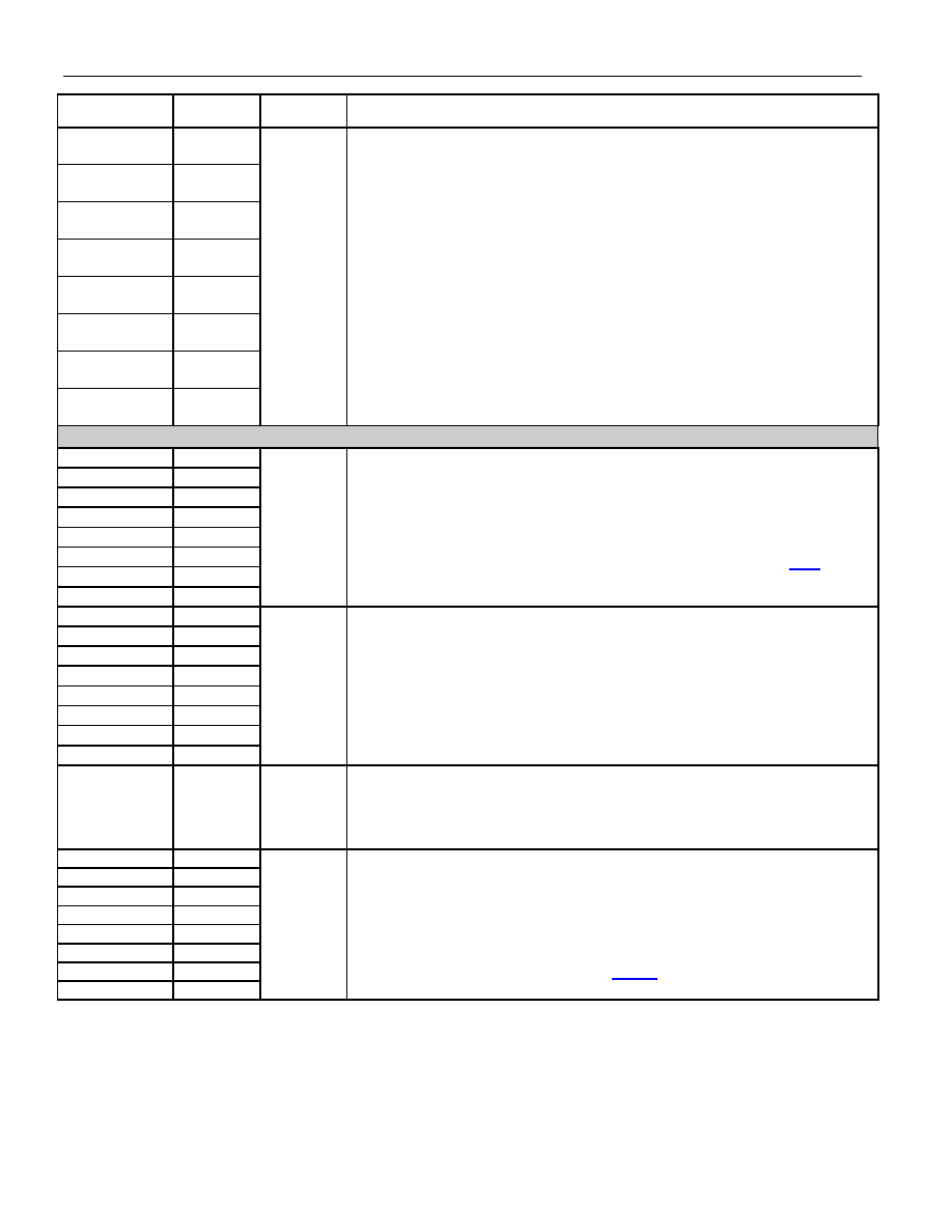
NAME
PIN
TYPE
FUNCTION
TCHBLK/
CLK1
A5
TCHBLK/
CLK2
C7
TCHBLK/
CLK3
L7
TCHBLK/
CLK4
P7
TCHBLK/
CLK5
P9
TCHBLK/
CLK6
P11
TCHBLK/
CLK7
D10
TCHBLK/
CLK8
E11
O
Transmit Channel Block/Transmit Channel Block Clock. A dual function pin.
TCHBLK is a user-programmable output that can be forced high or low during any
of the channels. It is synchronous with TCLK when the transmit-side elastic store is
disabled. It is synchronous with TSYSCLK when the transmit-side elastic store is
enabled. It is useful for blocking clocks to a serial UART or LAPD controller in
applications where not all channels are used such as Fractional T1, Fractional E1,
384kbps (H0), 768kbps, or ISDN-PRI. Also useful for locating individual channels
in drop-and-insert applications, for external per-channel loopback, and for per-
channel conditioning.
TCHCLK. TCHCLKn is a dual function pin that can output either a gapped clock or
a channel clock. In gapped clock mode, TCHCLKn is a N x 64kHz fractional clock
that is software programmable for 0 to 24 channels and the F-bit (T1) or 0 to 32
channels (E1). In channel clock mode, TCHCLKn is a 192kHz (T1) or 256kHz (E1)
clock that pulses high during the LSB of each channel. It is useful for parallel-to-
serial conversion of channel data. In either mode, TCHCLKn is synchronous with
TCLKn when the receive-side elastic store is disabled or it is synchronous with
TSYSCLKn when the receive-side elastic store is enabled. The mode of TCHCLK
is determined by the TGCLKEN bit in the TESCR register.
RECEIVE FRAMER
RSER1
E5
RSER2
D6
RSER3
N4
RSER4
N6
RSER5
M11
RSER6
M12
RSER7
B12
RSER8
F11
O
Received Serial Data. Received NRZ serial data. Updated on rising edges of
RCLK when the receive-side elastic store is disabled. Updated on the rising edges
of RSYSCLK when the receive-side elastic store is enabled.
When IBO mode is used, the RSER pins can output data for multiple framers. The
RSER data is synchronous to RSYSCLK. This is described in Section 8.8.2.
RCLK1
F4
RCLK2
G4
RCLK3
L4
RCLK4
M4
RCLK5
K13
RCLK6
J13
RCLK7
F13
RCLK8
E13
O
Receive Clock. A 1.544MHz (T1) or 2.048MHz (E1) clock that is used to clock
data through the receive-side framer. This clock is recovered from the signal at
RTIP and RRING. RSER data is output on the rising edge of RCLK. RCLK is used
to output RSER when the elastic store is not enabled or IBO is not used. When the
elastic store is enabled or IBO is used, the RSER is clocked by RSYSCLK.
RSYSCLK
L12
I
Receive System Clock. 1.544MHz, 2.048MHz, 4.096MHz, 8.192MHz, or
16.384MHz receive backplane clock. Only used when the receive-side elastic store
function is enabled. Should be tied low in applications that do not use the receive-
side elastic store. Multiple of 2.048MHz is expected when the IBO mode is used.
Note that RSYSCLK is used for all eight transceivers.
RSYNC1
A4
RSYNC2
B6
RSYNC3
N5
RSYNC4
T6
RSYNC5
R10
RSYNC6
P12
RSYNC7
C11
RSYNC8
D13
I/O
Receive Synchronization. If the receive-side elastic store is enabled, then this
signal is used to input a frame or multiframe boundary pulse. If set to output frame
boundaries, then RSYNC can be programmed to output double-wide pulses on
signaling frames in T1 mode. In E1 mode, RSYNC out can be used to indicate
CAS and CRC-4 multiframe. The DS26528 can accept H.100-compatible
synchronization signal. The default direction of this pin at power-up is input, as
determined by the RSIO control bit in the RIOCR.2 register.
相關(guān)PDF資料 |
PDF描述 |
|---|---|
| DS26324GNA3+ | IC LIU E1/T1/J1 3.3V 256-CSBGA |
| MAX1070CTC+ | IC ADC 10BIT 1.5MSPS 12-TQFN |
| DS21458N+ | IC LIU QUAD T1/E1/J1 256-CSBGA |
| DS3152+ | IC LIU DS3/E3/STS-1 144-CSBGA |
| VI-25H-IU-F2 | CONVERTER MOD DC/DC 52V 200W |
相關(guān)代理商/技術(shù)參數(shù) |
參數(shù)描述 |
|---|---|
| DS26528G+ | 功能描述:網(wǎng)絡(luò)控制器與處理器 IC 8-Port E1/T1/J1 Transceiver RoHS:否 制造商:Micrel 產(chǎn)品:Controller Area Network (CAN) 收發(fā)器數(shù)量: 數(shù)據(jù)速率: 電源電流(最大值):595 mA 最大工作溫度:+ 85 C 安裝風(fēng)格:SMD/SMT 封裝 / 箱體:PBGA-400 封裝:Tray |
| DS26528GA2 | 功能描述:網(wǎng)絡(luò)控制器與處理器 IC RoHS:否 制造商:Micrel 產(chǎn)品:Controller Area Network (CAN) 收發(fā)器數(shù)量: 數(shù)據(jù)速率: 電源電流(最大值):595 mA 最大工作溫度:+ 85 C 安裝風(fēng)格:SMD/SMT 封裝 / 箱體:PBGA-400 封裝:Tray |
| DS26528GA3 | 功能描述:網(wǎng)絡(luò)控制器與處理器 IC RoHS:否 制造商:Micrel 產(chǎn)品:Controller Area Network (CAN) 收發(fā)器數(shù)量: 數(shù)據(jù)速率: 電源電流(最大值):595 mA 最大工作溫度:+ 85 C 安裝風(fēng)格:SMD/SMT 封裝 / 箱體:PBGA-400 封裝:Tray |
| DS26528GA4 | 功能描述:網(wǎng)絡(luò)控制器與處理器 IC RoHS:否 制造商:Micrel 產(chǎn)品:Controller Area Network (CAN) 收發(fā)器數(shù)量: 數(shù)據(jù)速率: 電源電流(最大值):595 mA 最大工作溫度:+ 85 C 安裝風(fēng)格:SMD/SMT 封裝 / 箱體:PBGA-400 封裝:Tray |
| DS26528GA5 | 功能描述:網(wǎng)絡(luò)控制器與處理器 IC 8-Port E1/T1/J1 Transceiver RoHS:否 制造商:Micrel 產(chǎn)品:Controller Area Network (CAN) 收發(fā)器數(shù)量: 數(shù)據(jù)速率: 電源電流(最大值):595 mA 最大工作溫度:+ 85 C 安裝風(fēng)格:SMD/SMT 封裝 / 箱體:PBGA-400 封裝:Tray |
發(fā)布緊急采購(gòu),3分鐘左右您將得到回復(fù)。