- 您現(xiàn)在的位置:買賣IC網(wǎng) > PDF目錄9673 > DS26503L+ (Maxim Integrated Products)IC T1/E1/J1 BITS ELEMENT 64-LQFP PDF資料下載
參數(shù)資料
| 型號: | DS26503L+ |
| 廠商: | Maxim Integrated Products |
| 文件頁數(shù): | 29/122頁 |
| 文件大?。?/td> | 0K |
| 描述: | IC T1/E1/J1 BITS ELEMENT 64-LQFP |
| 產(chǎn)品培訓(xùn)模塊: | Lead (SnPb) Finish for COTS Obsolescence Mitigation Program |
| 標(biāo)準(zhǔn)包裝: | 160 |
| 類型: | BITS 元件,多路復(fù)用器 |
| PLL: | 是 |
| 主要目的: | T1/E1 |
| 輸入: | 時鐘 |
| 輸出: | 時鐘 |
| 電路數(shù): | 1 |
| 比率 - 輸入:輸出: | 2:2 |
| 差分 - 輸入:輸出: | 無/無 |
| 頻率 - 最大: | 6.312MHz |
| 電源電壓: | 3.135 V ~ 3.465 V |
| 工作溫度: | 0°C ~ 70°C |
| 安裝類型: | 表面貼裝 |
| 封裝/外殼: | 64-LQFP |
| 供應(yīng)商設(shè)備封裝: | 64-LQFP(10x10) |
| 包裝: | 托盤 |
| 產(chǎn)品目錄頁面: | 1430 (CN2011-ZH PDF) |
第1頁第2頁第3頁第4頁第5頁第6頁第7頁第8頁第9頁第10頁第11頁第12頁第13頁第14頁第15頁第16頁第17頁第18頁第19頁第20頁第21頁第22頁第23頁第24頁第25頁第26頁第27頁第28頁當(dāng)前第29頁第30頁第31頁第32頁第33頁第34頁第35頁第36頁第37頁第38頁第39頁第40頁第41頁第42頁第43頁第44頁第45頁第46頁第47頁第48頁第49頁第50頁第51頁第52頁第53頁第54頁第55頁第56頁第57頁第58頁第59頁第60頁第61頁第62頁第63頁第64頁第65頁第66頁第67頁第68頁第69頁第70頁第71頁第72頁第73頁第74頁第75頁第76頁第77頁第78頁第79頁第80頁第81頁第82頁第83頁第84頁第85頁第86頁第87頁第88頁第89頁第90頁第91頁第92頁第93頁第94頁第95頁第96頁第97頁第98頁第99頁第100頁第101頁第102頁第103頁第104頁第105頁第106頁第107頁第108頁第109頁第110頁第111頁第112頁第113頁第114頁第115頁第116頁第117頁第118頁第119頁第120頁第121頁第122頁
DS26503 T1/E1/J1 BITS Element
14 of 122
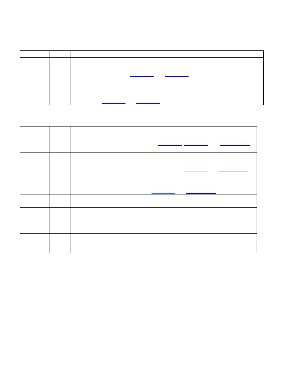
4. PIN FUNCTION DESCRIPTION
4.1 Transmit PLL
NAME
TYPE
FUNCTION
PLL_OUT
O
Transmit PLL Output. This pin can be selected to output the 1544kHz,
2048kHz, 64kHz, or 6312kHz output from the internal TX PLL or the internal
signal, TX CLOCK. See Figure 3-3 and Figure 3-4.
TCLK
I
Transmit Clock Input. A 64kHz, 1.544MHz, 2.048MHz, or 6312kHz primary
clock. May be selected by the TX PLL mux to either directly drive the transmit
section or be converted to one of the other rates prior to driving the transmit
section. See Figure 3-3 and Figure 3-4.
4.2 Transmit Side
NAME
TYPE
FUNCTION
TSER
I
Transmit Serial Data. Source of transmit data sampled on the falling edge of
(transmit timing diagram).
TS
I/O
TSYNC. When in input mode, this pin is sampled on the falling edge of TX
CLOCK (an internal signal) and a pulse at this pin will establish either frame or
multiframe boundaries for the transmit side. See Figure 3-1 and Figure 19-11.
In output mode, the pin is updated on the rising edge of TX CLOCK (an
internal signal) and can be programmed to output a frame or multiframe sync
pulse useful for aligning data. See Figure 3-1 and Figure 19-11.
TCLKO
O
Transmit Clock Output. Buffered clock that is used to clock data through the
transmit-side formatter (i.e., either TCLK or RCLK).
TPOSO
O
Transmit Positive-Data Output. In T1 or E1 mode, updated on the rising edge
of TCLKO with the bipolar data out of the transmit-side formatter. Can be
programmed to source NRZ data via the output-data format (IOCR1.0) control
bit. In 6312kHz mode, this pin is low.
TNEGO
O
Transmit Negative-Data Output. In T1 or E1 mode, updated on the rising
edge of TCLKO with the bipolar data out of the transmit-side formatter. In
6312kHz mode, this pin is low.
相關(guān)PDF資料 |
PDF描述 |
|---|---|
| V375C48M150BF | CONVERTER MOD DC/DC 48V 150W |
| CS3106A-18-57P | CONN PLUG 6POS STRAIGHT W/PINS |
| ADN2812ACPZ | IC CLOCK/DATA RECOVERY 32LFCSP |
| MS27467T25B19PA | CONN PLUG 19POS STRAIGHT W/PINS |
| ADN2817ACPZ | IC CLOCK/DATA RECOVERY 32-LFCSP |
相關(guān)代理商/技術(shù)參數(shù) |
參數(shù)描述 |
|---|---|
| DS26503L+ | 功能描述:計時器和支持產(chǎn)品 E1-T1-J1 Bits Element RoHS:否 制造商:Micrel 類型:Standard 封裝 / 箱體:SOT-23 內(nèi)部定時器數(shù)量:1 電源電壓-最大:18 V 電源電壓-最小:2.7 V 最大功率耗散: 最大工作溫度:+ 85 C 最小工作溫度:- 40 C 封裝:Reel |
| DS26503LN | 功能描述:計時器和支持產(chǎn)品 E1-T1-J1 Bits Element RoHS:否 制造商:Micrel 類型:Standard 封裝 / 箱體:SOT-23 內(nèi)部定時器數(shù)量:1 電源電壓-最大:18 V 電源電壓-最小:2.7 V 最大功率耗散: 最大工作溫度:+ 85 C 最小工作溫度:- 40 C 封裝:Reel |
| DS26503LN+ | 功能描述:計時器和支持產(chǎn)品 E1-T1-J1 Bits Element RoHS:否 制造商:Micrel 類型:Standard 封裝 / 箱體:SOT-23 內(nèi)部定時器數(shù)量:1 電源電壓-最大:18 V 電源電壓-最小:2.7 V 最大功率耗散: 最大工作溫度:+ 85 C 最小工作溫度:- 40 C 封裝:Reel |
| DS26504 | 制造商:Maxim Integrated Products 功能描述:T1/E1/J1 ENH BITS ELEMENT LQFP - Trays |
| DS26504_06 | 制造商:MAXIM 制造商全稱:Maxim Integrated Products 功能描述:T1/E1/J1/64KCC BITS Element |
發(fā)布緊急采購,3分鐘左右您將得到回復(fù)。