- 您現(xiàn)在的位置:買賣IC網(wǎng) > PDF目錄8993 > CY28329ZXCT (Silicon Laboratories Inc)IC CLOCK CK408B PLUMAS 56SSOP PDF資料下載
參數(shù)資料
| 型號(hào): | CY28329ZXCT |
| 廠商: | Silicon Laboratories Inc |
| 文件頁(yè)數(shù): | 14/16頁(yè) |
| 文件大?。?/td> | 0K |
| 描述: | IC CLOCK CK408B PLUMAS 56SSOP |
| 標(biāo)準(zhǔn)包裝: | 2,000 |
| 類型: | * |
| PLL: | 是 |
| 輸入: | 晶體 |
| 輸出: | 時(shí)鐘 |
| 電路數(shù): | 1 |
| 比率 - 輸入:輸出: | 1:24 |
| 差分 - 輸入:輸出: | 無(wú)/是 |
| 頻率 - 最大: | 133MHz |
| 除法器/乘法器: | 無(wú)/無(wú) |
| 電源電壓: | 3.135 V ~ 3.465 V |
| 工作溫度: | 0°C ~ 70°C |
| 安裝類型: | * |
| 封裝/外殼: | * |
| 供應(yīng)商設(shè)備封裝: | * |
| 包裝: | * |
| 其它名稱: | SLCY28329ZXCT |
第1頁(yè)第2頁(yè)第3頁(yè)第4頁(yè)第5頁(yè)第6頁(yè)第7頁(yè)第8頁(yè)第9頁(yè)第10頁(yè)第11頁(yè)第12頁(yè)第13頁(yè)當(dāng)前第14頁(yè)第15頁(yè)第16頁(yè)
CY28329
....................... Document #: 38-07040 Rev. *E Page 7 of 16
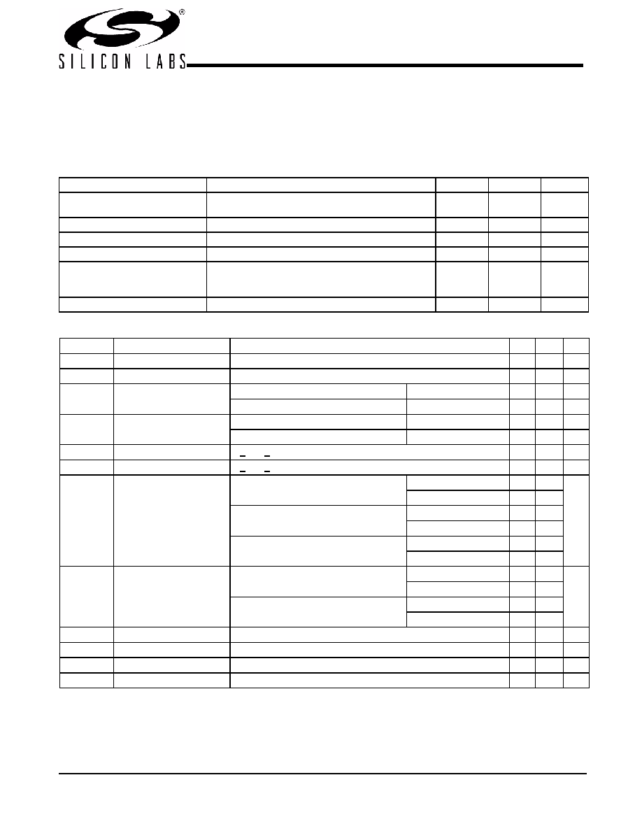
Absolute Maximum Conditions
(Above which the useful life may be impaired. For user guide-
lines, not tested.)
Supply Voltage..................................................–0.5 to +7.0V
Input Voltage............................................ –0.5V to VDD + 0.5
Storage Temperature (Non-Condensing) ....–65°C to +150°C
Max. Soldering Temperature (10 sec.) ...................... +260°C
Junction Temperature................................................ +150°C
Package Power Dissipation.............................................. 1W
Static Discharge Voltage ........................................................
(per MIL-STD-883, Method 3015) ............................ > 2000V
Operating Conditions over which electrical parameters are guaranteed[7]
Parameter
Description
Min.
Max.
Unit
VDD_REF, VDD_PCI,VDD_CORE,
VDD_3V66, VDD_48 MHz, VDD_CPU,
3.3V Supply Voltages
3.135
3.465
V
TA
Operating Temperature, Ambient
0
70
C
Cin
Input Pin Capacitance
5
pF
CXTAL
XTAL Pin Capacitance
22.5
pF
CL
Max. Capacitive Load on
USBCLK, REF
PCICLK, 3V66
20
30
pF
f(REF)
Reference Frequency, Oscillator Nominal Value
14.318
MHz
DC Electrical Specifications Over the Operating Range
Parameter
Description
Test Conditions
Min. Max. Unit
VIH
High-level Input Voltage
Except Crystal Pads. Threshold voltage for crystal pads = VDD/2
2.0
V
VIL
Low-level Input Voltage
Except Crystal Pads
0.8
V
VOH
High-level Output Voltage
USB, REF, 3V66
IOH = –1 mA
2.4
V
PCI
IOH = –1 mA
2.4
V
VOL
Low-level Output Voltage
USB, REF, 3V66
IOL = 1 mA
0.4
V
PCI
IOL = 1 mA
0.55
V
IIH
Input High Current
0 < VIN < VDD
–5
5
mA
IIL
Input Low Current
0 < VIN < VDD
–5
5
mA
IOH
High-level Output Current
CPU
For IOH =6*IRef Configuration
Type X1, VOH = 0.65V
12.9
mA
Type X1, VOH = 0.74V
14.9
REF, DOT, USB
Type 3, VOH = 1.00V
–29
Type 3, VOH = 3.135V
–23
3V66, DOT, PCI
Type 5, VOH = 1.00V
–33
Type 5, VOH = 3.135V
–33
IOL
Low-level Output Current
REF, DOT, USB
Type 3, VOL = 1.95V
29
mA
Type 3, VOL = 0.4V
27
3V66, PCI
Type 5, VOL =1.95 V
30
Type 5, VOL = 0.4V
38
IOZ
Output Leakage Current
Three-state
10
mA
IDD3
3.3V Power Supply Current VDD_CORE/VDD3.3 = 3.465V, FCPU = 133 MHz
360
mA
IDDPD3
3.3V Shutdown Current
VDD_CORE/VDD3.3 = 3.465V and @ IREF = 2.32 mA
25
mA
IDDPD3
3.3V Shutdown Current
VDD_CORE/VDD3.3 = 3.465V and @ IREF = 5.0 mA
45
mA
Note:
7. Multiple Supplies: the voltage on any input or I/O pin cannot exceed the power pin during power-up. Power supply sequencing is NOT required.
相關(guān)PDF資料 |
PDF描述 |
|---|---|
| CY28329OXCT | IC CLOCK CK408B PLUMAS 56SSOP |
| VE-J4L-MZ-F2 | CONVERTER MOD DC/DC 28V 25W |
| ADG3301BKSZ-REEL7 | TRANSLATOR SGL LL BIDIR SC70-6 |
| VE-J4L-MZ-F1 | CONVERTER MOD DC/DC 28V 25W |
| VI-24B-MY-F3 | CONVERTER MOD DC/DC 95V 50W |
相關(guān)代理商/技術(shù)參數(shù) |
參數(shù)描述 |
|---|---|
| CY2833 | 制造商:CYPRESS 制造商全稱:Cypress Semiconductor 功能描述:Intel CK408 Mobile Clock Synthesizer |
| CY28330 | 制造商:CYPRESS 制造商全稱:Cypress Semiconductor 功能描述:Clock Generator for AMD⑩ Hammer |
| CY28330OC | 制造商:Cypress Semiconductor 功能描述: |
| CY28330OCT | 制造商:CYPRESS 制造商全稱:Cypress Semiconductor 功能描述:Clock Generator for AMD⑩ Hammer |
| CY28331 | 制造商:CYPRESS 制造商全稱:Cypress Semiconductor 功能描述:Clock Generator for AMD⑩ Hammer |
發(fā)布緊急采購(gòu),3分鐘左右您將得到回復(fù)。