- 您現(xiàn)在的位置:買賣IC網(wǎng) > PDF目錄384267 > CXP402R 4-Bit Microcontroller PDF資料下載
參數(shù)資料
| 型號(hào): | CXP402R |
| 英文描述: | 4-Bit Microcontroller |
| 中文描述: | 4位微控制器 |
| 文件頁(yè)數(shù): | 4/16頁(yè) |
| 文件大小: | 262K |
| 代理商: | CXP402R |
第1頁(yè)第2頁(yè)第3頁(yè)當(dāng)前第4頁(yè)第5頁(yè)第6頁(yè)第7頁(yè)第8頁(yè)第9頁(yè)第10頁(yè)第11頁(yè)第12頁(yè)第13頁(yè)第14頁(yè)第15頁(yè)第16頁(yè)
– 4 –
CXP402
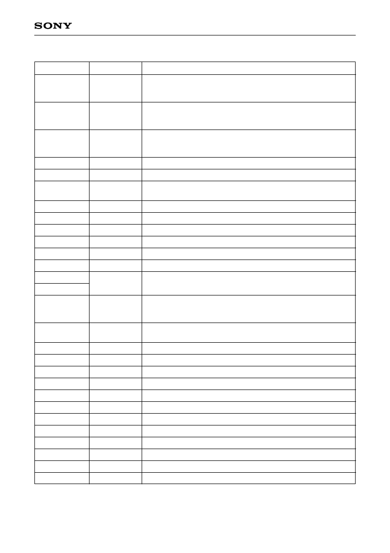
Pin Description
Symbol
I/O
Description
(Port A)
4-bit I/O port. I/O can be set in a unit of single bits. Pull-up resistor is
attached for input. (4 pins)
(Port B)
4-bit I/O port. I/O can be set in a unit of single bits. Pull-up resistor is
attached for input. (4 pins)
(Port C)
4-bit I/O port. I/O can be set in a unit of single bits. Pull-up resistor is
attached for input. (4 pins)
LCD segment signal output. (16 pins)
LCD common signal output.
LCD bias power supply. Bias voltage is generated, which is 1/3 the
supply voltage due to the internal resistor. (3 pins)
SENS input from SSP.
Track jump count signal input.
Serial data output to SSP.
Serial data latch output to SSP.
Serial clock output to SSP.
Spindle motor ON/OFF control output.
Spindle motor servo control. (2 pins)
Lock signal output. GFS is sampled at 460Hz and; when GFS is high,
this pin outputs a high signal. If GFS is low eight convective samples,
this pin outputs low.
Wide-band EFM PLL charge pump output. (2 pins)
Wide-band EFM PLL VCO2 oscillation input.
Wide-band EFM PLL VCO2 oscillation output.
Wide-band EFM PLL VCO2 control voltage input.
Master PLL charge pump output.
Master PLL filter input.
Master PLL filter output.
Master VCO control voltage input.
EFM signal input.
Asymmetry circuit constant current input.
Asymmetry comparator voltage input.
EFM output. (full swing)
System reset input. Active at low.
I/O
I/O
I/O
Output
Output
Input
Input
Output
Output
Output
Output
Output
(tri-state)
Output
Output
(tri-state)
Input
Output
Input
Output (tri-state)
Input
Output (Analog)
Input
Input
Input
Input
Output
Input
PA0 to PA3
PB0 to PB3
PC0 to PC3
SEG0 to SEG15
COM0 to COM3
V
LC1
to V
LC3
SEIN
CNIN
DATO
XLTO
CLKO
MON
MDP
MDS
LOCK
VPCO1
VPCO2
VCKI
V16M
VCTL
PCO
FILI
FILO
CLTV
RF
BIAS
ASYI
ASYO
XRST
相關(guān)PDF資料 |
PDF描述 |
|---|---|
| CXP5116 | 4-Bit Microcontroller |
| CXP5116Q | 4-Bit Microcontroller |
| CXP5118 | 4-Bit Microcontroller |
| CXP5118Q | 4-Bit Microcontroller |
| CXP750064 | CMOS 8-bit Single Chip Microcomputer |
相關(guān)代理商/技術(shù)參數(shù) |
參數(shù)描述 |
|---|---|
| CXP-437 | 制造商:SYNERGY 制造商全稱:SYNERGY MICROWAVE CORPORATION 功能描述:MIXERS SUB-HARMONIC |
| CXP5010 | 制造商:未知廠家 制造商全稱:未知廠家 功能描述:4-Bit Microcontroller |
| CXP50100 | 制造商:SONY 制造商全稱:Sony Corporation 功能描述:CMOS 4-BIT 1 CHIP MICROCOMPUTER |
| CXP50100-U01Q | 制造商:未知廠家 制造商全稱:未知廠家 功能描述:4-Bit Microcontroller |
| CXP5010H-P02AS | 制造商:未知廠家 制造商全稱:未知廠家 功能描述:4-Bit Microcontroller |
發(fā)布緊急采購(gòu),3分鐘左右您將得到回復(fù)。