- 您現(xiàn)在的位置:買賣IC網(wǎng) > PDF目錄223633 > CX77304-16 (SKYWORKS SOLUTIONS INC) 2MM SOCKET STRIPS PDF資料下載
參數(shù)資料
| 型號(hào): | CX77304-16 |
| 廠商: | SKYWORKS SOLUTIONS INC |
| 元件分類: | 放大器 |
| 英文描述: | 2MM SOCKET STRIPS |
| 中文描述: | 880 MHz - 915 MHz RF/MICROWAVE NARROW BAND MEDIUM POWER AMPLIFIER |
| 封裝: | 9.10 X 11.60 MM, 1.50 MM HEIGHT, LEAD FREE, PLASTIC, LEADLESS, SO-16 |
| 文件頁數(shù): | 7/18頁 |
| 文件大?。?/td> | 1089K |
| 代理商: | CX77304-16 |
PA MODULE FOR TRI-BAND EGSM DCS PCS / GPRS
DATA SHEET CX77304-16
Skyworks Solutions, Inc. Phone [781] 376-3000 Fax [781] 376-3100 sales@skyworksinc.com www.skyworksinc.com
101944B Skyworks Proprietary and Confidential Information Products and Product Information are Subject to Change Without Notice. July 28, 2004
15
Standby Mode Control
The Combinational Logic cell includes enable circuitry that
monitors the APC ramping voltage from the power amplifier
controller (PAC) circuit in the GSM transmitter. Typical handset
designs directly connect the PA VCC to the battery at all times, and
for some PA manufacturers this requires a control signal to set
the device in or out of standby mode. The Skyworks PAM does
not require a Transmit Enable input because it contains a standby
detection circuit that senses the VAPC to enable or disable the PA.
This feature helps minimize battery discharge when the PA is in
standby mode. When VAPC is below the enable threshold voltage,
the PA goes into a standby mode, which reduces battery current
(ICC) to 6
A, typical, under nominal conditions.
For voltages less than 700 mV at the APC input (pin 14), the PA
bias is held at ground. As the APC input exceeds the enable
threshold, the bias will activate. After an 8
s delay, the amplifier
internal bias will ramp quickly to match the ramp voltage applied
to the APC input. In order for the internal bias to precisely follow
the APC ramping voltage, it is critical that a ramp pedestal is set
to the APC input at or above the enable threshold level with a
timing at least 8
s prior to ramp-up. This will be discussed in
more detail in the following section, “Power Ramping
Considerations for 3GPP Compliance”.
Band Select
The Combinational Logic cell also includes a simple gate
arrangement that selects the desired operational band by
activating the appropriate current buffer. The voltage threshold
level at the Band Select input (pin 16) will determine the active
path of the bias output to the GaAs die.
Voltage Clamp
The Voltage Clamp circuit will limit the maximum bias voltage
output applied to the bases of the HBT devices on the GaAs die.
This provides protection against electrical overstress (EOS) of the
active devices during high voltage and/or load mismatch
conditions. Figure 11 shows the typical transfer function of the
APC input to buffer output under resistively loaded conditions.
Notice the enable function near 600 mV, and the clamp acting at
2.15 V, corresponding to a supply voltage of 4.0 V.
Figure 11. Base Bias Voltage vs. APC Input, VCC = 4.0 V
Due to output impedance effects, the bias of the GaAs devices
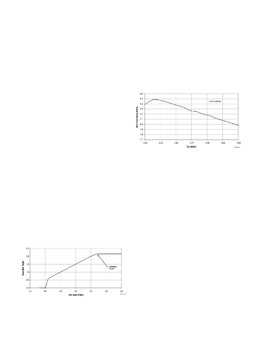
increases as the supply voltage increases. The Voltage Clamp is
designed to gradually decrease in level as the battery voltage
increases. The performance of the clamp circuit is enhanced by
the band gap reference that provides a supply-, process-, and
temperature-independent reference voltage. The transfer function
relative to VBAT is shown in Figure 12. For battery voltages below
3.4 V, the base bias voltage is limited by the common mode range
of the buffer amplifier. For battery voltages above 3.4 V, the
clamp limits the base bias.
Figure 12. Base Bias Clamp Voltage vs. Supply Voltage
Current Buffer
The output buffer amplifier performs a vital function in the CMOS
device by transferring the APC input voltage ramp to the base of
the GaAs power devices. This allows the APC input to be a high
impedance port, sinking only 10
A, typical, assuring no loading
effects on the PAC circuit. The buffers are designed to source the
high GaAs base currents required, while allowing a settling time
of less than 8
s for a 1.5 V ramp.
Power Ramping Considerations for 3GPP Compliance
The primary variables in the power control loop that the system
designer must control are:
Software control of the DSP / DAC
Software control of the transmitter timing signals
Ramp profile attributes - pedestal, number of steps, duration of
steps
Layout of circuit / parasitics
RC time constants within the PAC circuit design
All of these variables will directly influence the ability of a GSM
transmitter power control loop to comply with 3GPP
specifications.
Although there is a specific time mask template in which the
transmitter power is allowed to ramp up, the method is very
critical. The 3GPP system specification for switching transients
results in a requirement to limit the edge rate of output power
相關(guān)PDF資料 |
PDF描述 |
|---|---|
| CX77304-17 | YTQ-125-01-L-Q 2MM STACK OCTOPUS AUG 22/02 HI DENSITY STACKER |
| CX805-30 | CX805-30 Baseband Processor for Multiband GSM and GPRS Applications |
| CXA10-48D05 | 2-OUTPUT 10 W DC-DC REG PWR SUPPLY MODULE |
| CXA1786N-T4 | PHASE LOCKED LOOP, 1100 MHz, PDSO20 |
| CXD5-15 | 2-OUTPUT DC-DC REG PWR SUPPLY MODULE |
相關(guān)代理商/技術(shù)參數(shù) |
參數(shù)描述 |
|---|---|
| CX77304-17 | 制造商:SKYWORKS 制造商全稱:SKYWORKS 功能描述:CX77304-17 PA Module for Tri-band EGSM DCS PCS / GPRS |
| CX77306-11P | 制造商:Cypress Semiconductor 功能描述:CX77306-11P 制造商:Skyworks Solutions Inc 功能描述:CX77306-11P |
| CX77312 | 制造商:未知廠家 制造商全稱:未知廠家 功能描述:CX77312 Product Summary|PA Modules for GSM/GPRS Handsets |
| CX77314 | 制造商:未知廠家 制造商全稱:未知廠家 功能描述:CX77314 Product Summary|PA Modules for GSM/GPRS Handsets |
| CX77315 | 制造商:未知廠家 制造商全稱:未知廠家 功能描述:CX77315 Product Summary|PA Modules for GSM/GPRS Handsets |
發(fā)布緊急采購,3分鐘左右您將得到回復(fù)。