- 您現(xiàn)在的位置:買賣IC網(wǎng) > PDF目錄223633 > CX72301-11 (SKYWORKS SOLUTIONS INC) PLL FREQUENCY SYNTHESIZER, 1000 MHz, PDSO28 PDF資料下載
參數(shù)資料
| 型號: | CX72301-11 |
| 廠商: | SKYWORKS SOLUTIONS INC |
| 元件分類: | PLL合成/DDS/VCOs |
| 英文描述: | PLL FREQUENCY SYNTHESIZER, 1000 MHz, PDSO28 |
| 封裝: | EXPOSED PAD, TSSOP-28 |
| 文件頁數(shù): | 5/20頁 |
| 文件大?。?/td> | 165K |
| 代理商: | CX72301-11 |
DATA SHEET CX72301
Skyworks Solutions, Inc. Phone [781] 376-3000 Fax [781] 376-3100 sales@skyworksinc.com www.skyworksinc.com
101090H Skyworks Proprietary and Confidential information Products and Product Information are Subject to Change Without Notice July 21, 2004
13
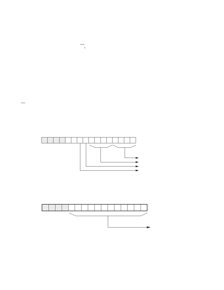
The Modulation Control Register is used to configure the
modulation unit of the main synthesizer. The modulation unit adds
or subtracts a frequency offset to the selected center frequency at
which the main synthesizer operates. The size of the modulation
data sample, controlled by the duration of the CS signal, can be
from 2 to 12 bits wide, to provide from 4 to 4096 selectable
frequency offset steps.
The modulation data magnitude offset selects the magnitude
multiplier for the modulation data and can be from 0 to 8. As
shown in Figure 14, the values to be loaded are:
Modulation Data Magnitude Offset = 4-bit value that indicates
the magnitude multiplier (m) for the modulation data samples.
Valid values range from 0 to 13, effectively providing a 2m
multiplication of the modulation data sample.
Modulation Data Input Select = 1-bit value that indicates the pin
on which modulation data samples are serially input when the
CS signal is between 2 and 12 bits long. When this bit is 0,
modulation data samples are to be presented on the Data pin.
When this bit is 1, modulation data samples are to be presented
on the Mod_in pin.
Modulation Address Disable = 1-bit value that indicates the
presence of the address as modulation data samples are
presented on either the Mod_in or Data pins. When this bit is 0,
the address is presented with the modulation data samples (i.e.,
all transfers are 16 bits long). When this bit is 1, no address is
presented with the modulation data samples (i.e., all transfers
are 2 to 12 bits long).
The Modulation Data Register is used to load the modulation data
samples to the modulation unit. This value is transferred to the
modulation unit on the falling edge of Fpd_main where it is passed to
the main
Σ modulator at the selected magnitude offset on the
next falling edge of Fpd_main. Modulation Data register values are
2's complement format. As shown in Figure 15, the value to be
loaded is:
Modulation Data Bits = Modulation data samples that represent
the desired instantaneous frequency offset to the selected main
synthesizer frequency (selected channel) before being affected
by the modulation data magnitude offset.
A3
A2 A1
A0 11
10
9
8
7
6
5
4
3
2
1
0
1
0
00
0
X
Reserved Bits
Modulation Data Magnitude Offset
Modulation Data Input Select
Modulation Address Disable
C1425
Figure 14. Modulation Control Register (Write Only)
A3
A2 A1
A0 11
10
9
8
7
6
5
4
3
2
1
0
10
01 MSB
LSB
Modulation Data Bits
C1426
Figure 15. Modulation Data Register (Write Only)
相關(guān)PDF資料 |
PDF描述 |
|---|---|
| CX74017 | On the Direct Conversion Receiver |
| CX74038-12 | 2.6 GHz/800 MHz Dual Fractional-N/lnteger-N Frequency Synthesizer |
| CX77105-16P | Power Amplifier Module for CDMA/AMPS (824-849 MHz) |
| CX77107-14P | PA Module for CDMA / PCS (1850-1910 MHz) |
| CX77304-15 | 2MM SOCKET STRIPS |
相關(guān)代理商/技術(shù)參數(shù) |
參數(shù)描述 |
|---|---|
| CX72302 | 制造商:未知廠家 制造商全稱:未知廠家 功能描述:CX72302: Spur-Free, 6.1 GHz Dual Fractional-N Frequency Synthesizer |
| CX72303 | 制造商:未知廠家 制造商全稱:未知廠家 功能描述:CX72303 1.8 V Ultra Low Power Bluetooth? RF Tx|Bluetooth? RF Transceiver |
| CX725 2HDG | 制造商:Thomas & Betts 功能描述:EXTENDED PIPE CLAMP |
| CX7352-000 | 制造商:TE Connectivity 功能描述:RT-1145-OX-29-0-CS6450 - Bag |
| CX7354-000 | 制造商:TE Connectivity 功能描述:D-436-83CS2621 |
發(fā)布緊急采購,3分鐘左右您將得到回復(fù)。