- 您現(xiàn)在的位置:買賣IC網(wǎng) > PDF目錄373032 > BUK542-100B (NXP SEMICONDUCTORS) PowerMOS transistor Logic level FET PDF資料下載
參數(shù)資料
| 型號(hào): | BUK542-100B |
| 廠商: | NXP SEMICONDUCTORS |
| 元件分類: | JFETs |
| 英文描述: | PowerMOS transistor Logic level FET |
| 中文描述: | 5.6 A, 100 V, 0.35 ohm, N-CHANNEL, Si, POWER, MOSFET |
| 封裝: | PLASTIC, FULL PACK-3 |
| 文件頁(yè)數(shù): | 2/8頁(yè) |
| 文件大小: | 58K |
| 代理商: | BUK542-100B |
Philips Semiconductors
Product Specification
PowerMOS transistor
Logic level FET
BUK542-100A/B
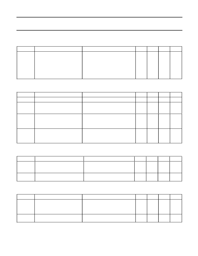
STATIC CHARACTERISTICS
T
hs
= 25 C unless otherwise specified
SYMBOL
PARAMETER
V
(BR)DSS
Drain-source breakdown
voltage
V
GS(TO)
Gate threshold voltage
I
DSS
Zero gate voltage drain current
I
DSS
Zero gate voltage drain current
I
GSS
Gate source leakage current
R
DS(ON)
Drain-source on-state
resistance
CONDITIONS
V
GS
= 0 V; I
D
= 0.25 mA
MIN.
100
TYP.
-
MAX.
-
UNIT
V
V
DS
= V
; I
= 1 mA
V
DS
= 100 V; V
GS
= 0 V; T
j
= 25 C
V
DS
= 100 V; V
GS
= 0 V; T
j
=125 C
V
GS
=
±
15 V; V
DS
= 0 V
V
GS
= 5 V;
I
D
1.0
-
-
-
-
-
1.5
1
0.1
10
0.25
0.3
2.0
10
1.0
100
0.28
0.35
V
μ
A
mA
nA
BUK542-100A
BUK542-100B
DYNAMIC CHARACTERISTICS
T
hs
= 25 C unless otherwise specified
SYMBOL
PARAMETER
g
fs
Forward transconductance
C
iss
Input capacitance
C
oss
Output capacitance
C
rss
Feedback capacitance
t
d on
Turn-on delay time
t
r
Turn-on rise time
t
d off
Turn-off delay time
t
f
Turn-off fall time
L
d
Internal drain inductance
CONDITIONS
V
DS
= 25 V; I
D
= 5.5 A
V
GS
= 0 V; V
DS
= 25 V; f = 1 MHz
MIN.
4.5
-
-
-
-
-
-
-
-
TYP.
6
400
90
35
12
45
50
30
4.5
MAX.
-
600
120
50
18
70
70
45
-
UNIT
S
pF
pF
pF
ns
ns
ns
ns
nH
V
DD
= 30 V; I
D
= 3 A;
V
GS
= 5 V; R
GS
= 50
;
R
gen
= 50
Measured from drain lead 6 mm
from package to centre of die
Measured from source lead 6 mm
from package to source bond pad
L
s
Internal source inductance
-
7.5
-
nH
ISOLATION LIMITING VALUE & CHARACTERISTIC
T
hs
= 25 C unless otherwise specified
SYMBOL
PARAMETER
V
isol
Repetitive peak voltage from all
three terminals to external
heatsink
C
isol
Capacitance from T2 to external f = 1 MHz
heatsink
CONDITIONS
R.H.
≤
65% ; clean and dustfree
MIN.
-
TYP.
MAX.
1500
UNIT
V
-
12
-
pF
REVERSE DIODE LIMITING VALUES AND CHARACTERISTICS
T
hs
= 25 C unless otherwise specified
SYMBOL
PARAMETER
I
DR
Continuous reverse drain
current
I
DRM
Pulsed reverse drain current
V
SD
Diode forward voltage
t
rr
Reverse recovery time
Q
rr
Reverse recovery charge
CONDITIONS
-
MIN.
-
TYP.
-
MAX.
6.3
UNIT
A
-
I
F
= 6.3 A ; V
GS
= 0 V
I
F
= 6.3 A; -dI
/dt = 100 A/
μ
s;
V
GS
= 0 V; V
R
= 30 V
-
-
-
-
-
25
1.5
-
-
A
V
ns
μ
C
1.2
80
0.30
April 1993
2
Rev 1.100
相關(guān)PDF資料 |
PDF描述 |
|---|---|
| BUK542-60A | PowerMOS transistor Logic level FET |
| BUK542-60B | PowerMOS transistor Logic level FET |
| BUK543-100A | PowerMOS transistor Logic level FET |
| BUK543-100B | PowerMOS transistor Logic level FET |
| BUK545-200A | PowerMOS transistor Logic level FET |
相關(guān)代理商/技術(shù)參數(shù) |
參數(shù)描述 |
|---|---|
| BUK542-50A | 制造商:未知廠家 制造商全稱:未知廠家 功能描述:N-Channel Enhancement MOSFET |
| BUK542-50B | 制造商:未知廠家 制造商全稱:未知廠家 功能描述:N-Channel Enhancement MOSFET |
| BUK542-60A | 制造商:PHILIPS 制造商全稱:NXP Semiconductors 功能描述:PowerMOS transistor Logic level FET |
| BUK542-60B | 制造商:PHILIPS 制造商全稱:NXP Semiconductors 功能描述:PowerMOS transistor Logic level FET |
| BUK543-100A | 制造商:PHILIPS 制造商全稱:NXP Semiconductors 功能描述:PowerMOS transistor Logic level FET |
發(fā)布緊急采購(gòu),3分鐘左右您將得到回復(fù)。