- 您現(xiàn)在的位置:買(mǎi)賣(mài)IC網(wǎng) > PDF目錄97843 > AWL6951RM22P8 (ANADIGICS INC) 2400 MHz - 2500 MHz RF/MICROWAVE NARROW BAND MEDIUM POWER AMPLIFIER PDF資料下載
參數(shù)資料
| 型號(hào): | AWL6951RM22P8 |
| 廠商: | ANADIGICS INC |
| 元件分類(lèi): | 放大器 |
| 英文描述: | 2400 MHz - 2500 MHz RF/MICROWAVE NARROW BAND MEDIUM POWER AMPLIFIER |
| 封裝: | 4 X 4 MM, 1.3 MM HEIGHT, ROHS COMPLIANT, M22, 16 PIN |
| 文件頁(yè)數(shù): | 12/22頁(yè) |
| 文件大?。?/td> | 951K |
| 代理商: | AWL6951RM22P8 |
第1頁(yè)第2頁(yè)第3頁(yè)第4頁(yè)第5頁(yè)第6頁(yè)第7頁(yè)第8頁(yè)第9頁(yè)第10頁(yè)第11頁(yè)當(dāng)前第12頁(yè)第13頁(yè)第14頁(yè)第15頁(yè)第16頁(yè)第17頁(yè)第18頁(yè)第19頁(yè)第20頁(yè)第21頁(yè)第22頁(yè)
2
Data Sheet - Rev 2.1
09/2007
AWL6951
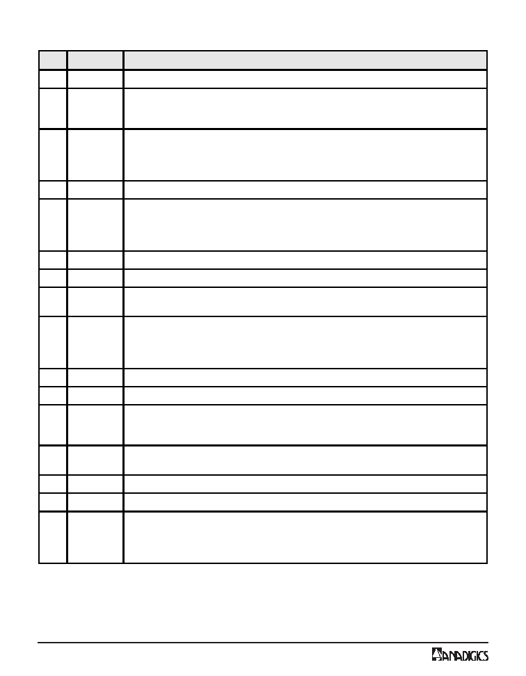
Table 1: Pin Description
PIN
NAME
DESCRIPTION
1
GND
Ground
2
RFIN 2G
2 GHz RF Input. ESD structures on this pin provide a DC path to ground. Avoid
applying DC voltage to this pin. RF is internally matched to 50 and AC coupled to
the input stage. Route RF traces as coplanar waveguide using adjacent ground pins.
3
RFIN 5G
5 GHz RF Input. AC coupled input stage internally matched to 50 . Route as coplanar
waveguide using adjacent ground pins. Although the input stage is AC coupled, a
shunt inductive matching element included inside the PA provides a DC path to ground
at this pin.
4
GND
Ground
5
PAON 5G
5 GHz Power Control. Power amplifier power control pin. The recommended use is for
on/off control of the PA. Nominally, 0 V applied will turn amplifier completely off; a
voltage of 2.0 V and above will set the PA to maximum output capability. Current draw
on this pin is approximately 0.5 mA at +3.3 V.
6
GND
Ground
7
VCC 5G
5 GHz Supply Voltage. Bias for power transistors of the 5 GHz PA.
8
DETOUT 5G 5 GHz Power Detector Output. DC coupled power detector output. An emitter follower
BJT supplies the output for this pin. Output impedance is 2 k.
9
RFOUT 5G
5 GHz RF Output. AC coupled output stage internally matched to 50 . Route as
coplanar waveguide using adjacent ground pins. Although the output stage is AC
coupled, a shunt inductive matching element included inside the PA provides a DC
path to ground at this pin.
10
GND
Ground
11
GND
Ground
12
RFOUT 2G
2 GHz RF Output. ESD structures on this pin provide a DC path to ground. Avoid
applying DC voltage to this pin. RF is internally matched to 50 and AC coupled to
the output stage. Route RF traces as coplanar waveguide using adjacent ground pins.
13
DETOUT 2G 2 GHz Power Detector Output. DC coupled power detector output. An emitter follower
BJT supplies the output for this pin. Output impedance is 2 k.
14
VCC 2G
2 GHz Power Supply. Bias for power transistors of the 2 GHz PA.
15
GND
Ground
16
PAON 2G
2 GHz Power Control. Power amplifier power control pin. The recommended use is for
on/off control of the PA. Nominally, 0 V applied will turn amplifier completely off; a
voltage of 2.0 V and above will set the PA to maximum output capability. Current draw
on this pin is approximately 0.5 mA at +3.3 V.
相關(guān)PDF資料 |
PDF描述 |
|---|---|
| AWL9925RD1P5 | 2400 MHz - 2500 MHz RF/MICROWAVE NARROW BAND MEDIUM POWER AMPLIFIER |
| AWL9925RD1Q4 | 2400 MHz - 2500 MHz RF/MICROWAVE NARROW BAND MEDIUM POWER AMPLIFIER |
| AWM6422RM18P8 | 2300 MHz - 2400 MHz RF/MICROWAVE NARROW BAND MEDIUM POWER AMPLIFIER |
| AWT6225RM26P8 | 880 MHz - 915 MHz RF/MICROWAVE NARROW BAND HIGH POWER AMPLIFIER |
| AWT6225RM26P9 | 880 MHz - 915 MHz RF/MICROWAVE NARROW BAND HIGH POWER AMPLIFIER |
相關(guān)代理商/技術(shù)參數(shù) |
參數(shù)描述 |
|---|---|
| AWL80/112/G | 制造商:Assmann Electronics Inc 功能描述: |
| AWL80/112/Z | 制造商:Assmann Electronics Inc 功能描述: |
| AWL80/118/G | 制造商:Assmann Electronics Inc 功能描述: |
| AWL9224 | 制造商:ANADIGICS 制造商全稱(chēng):ANADIGICS, Inc 功能描述:2.4 GHz 802.11b/g WLAN Power Amplifier |
| AWL9224_12 | 制造商:ANADIGICS 制造商全稱(chēng):ANADIGICS, Inc 功能描述:2.4 GHz 802.11b/g WLAN Power Amplifier |
發(fā)布緊急采購(gòu),3分鐘左右您將得到回復(fù)。