- 您現(xiàn)在的位置:買賣IC網(wǎng) > PDF目錄1902 > AS8530-ASOT-002-500 (ams)IC TXRX LIN COMPANION 8-SOIC PDF資料下載
參數(shù)資料
| 型號(hào): | AS8530-ASOT-002-500 |
| 廠商: | ams |
| 文件頁數(shù): | 32/33頁 |
| 文件大小: | 0K |
| 描述: | IC TXRX LIN COMPANION 8-SOIC |
| 標(biāo)準(zhǔn)包裝: | 500 |
| 系列: | * |
第1頁第2頁第3頁第4頁第5頁第6頁第7頁第8頁第9頁第10頁第11頁第12頁第13頁第14頁第15頁第16頁第17頁第18頁第19頁第20頁第21頁第22頁第23頁第24頁第25頁第26頁第27頁第28頁第29頁第30頁第31頁當(dāng)前第32頁第33頁
Revision 1.1
7 - 32
AS8530
Datasheet - Electrical Character i s t ics
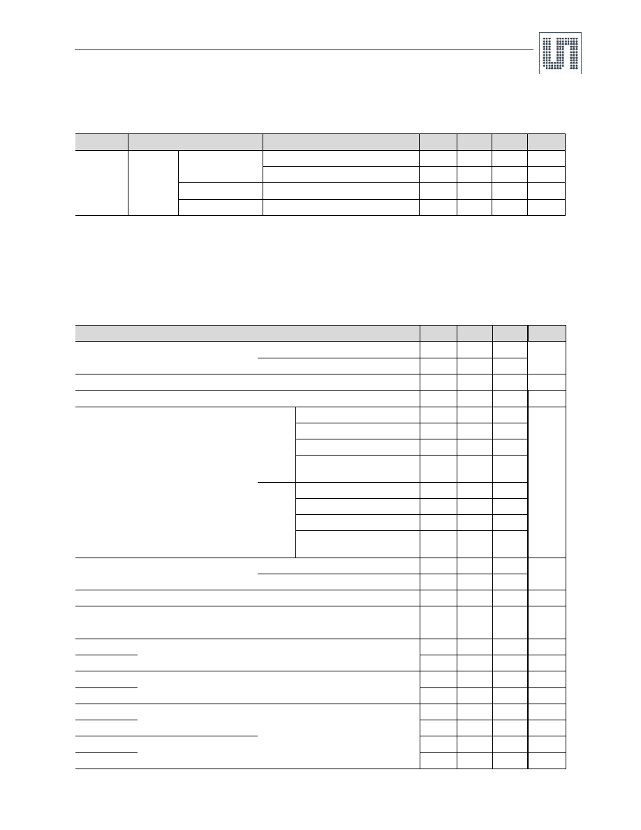
6.3 Detailed System and Block Specifications
6.3.1 Electrical System Specifications
6.4 Low Dropout Regulator
The LDO block is a linear voltage regulator, which provides a regulated (band-gap stabilized) output voltage (VCC) from the battery supply
voltage (VSUP).
(6V < VSUP < 18V for option 1, 6V <VSUP <18V option2; -40°C < TJ < 150°C; all voltages are with respect to ground (VSS); positive current
flows into the pin), normal operating mode if not otherwise mentioned.
Symbol
Parameter
Conditions
Min
Typ
Max
Units
IDDnom
1
1. No external load on the LIN bus
Current
consumption
Normal mode
No load on VCC, LIN recessive, VSUP= 12V
300
A
No load on VCC, LIN dominant, VSUP = 12V
700
A
Stand-by mode
Up to 125°C ambient (no load), VSUP= 12V
45
A
Sleep mode
Up to 125°C ambient (no load), VSUP=12V
35
A
Symbol
Parameter
Conditions
Min
Typ
Max
Units
VCC
Regulated supply voltage
ILOAD 0mA to 50mA
Option 1
4.75
5.25
V
Option 2
3.135
3.465
TJ
Junction Temperature
-40
150
C
VSUP
Supply Voltage Range
612
18
V
VCC
Output Voltage Range
Option 1
Load < 50mA
4.75
5.0
5.25
V
50mA to 65mA
4.5
5.5
Standby mode @ ICC < 5mA
4.5
5.5
Load-dump condition,
ILOAD < 50mA
5.5
Option 2
Load < 50mA
3.135
3.3
3.465
50mA to 65mA
2.97
3.3
3.63
Standby mode @ ICC < 5mA
2.97
3.63
Load-dump condition,
ILOAD < 50mA
3.63
ICC_SH
Output Short Circuit Current
Normal mode
50
250
mA
Standby mode
5
250
dVCC1
Line Regulation
ΔVCC / ΔVSUP
8mV/V
LOREG_SM
Load Regulation (Standby mode)
ΔVCC / ΔICCn (for ILOAD > 500A)
10
mV/mA
LOREG_NM
Load Regulation (Normal mode)
ΔVCC / ΔICCn (for ILOAD > 500A)
1
mV/mA
CL1
Output Capacitor (Electrolytic)
2.2
10
F
ESR1
110
Ω
CL2
Output Capacitor (Ceramic)
100
220
nF
ESR2
0.02
1
Ω
CSUP1E
Input capacitor (Electrolytic)
For EMC suppression
10
100
F
ESR1_CSUP
110
Ω
CSUP2C
Input capacitor (Ceramic)
100
220
nF
ESR2_CSUP
0.02
1
Ω
相關(guān)PDF資料 |
PDF描述 |
|---|---|
| AS8530A-ASOT-500 | IC SYSTEM BASIS CHIP 8-SOIC |
| AT17F080-30TQI | IC FLASH CONFIG 8M 44TQFP |
| AT17F080A-30QI | IC FLASH CONFIG 8M 32TQFP |
| AT17F16-30TQI | IC FLASH CONFIG 16M 44TQFP |
| AT17F16A-30JU | IC FLASH CONFIG 16M 20PLCC |
相關(guān)代理商/技術(shù)參數(shù) |
參數(shù)描述 |
|---|---|
| AS8530-ASOT-500 | 制造商:ams 功能描述: |
| AS8578-A | 制造商:Coilcraft Inc 功能描述:DSL transformer, for TI TNETDx000R, not RoHS |
| AS8579-A | 制造商:Coilcraft Inc 功能描述:DSL transformer, for TI TNETDx000R, SMT, not RoHS |
| AS8580 | 制造商:未知廠家 制造商全稱:未知廠家 功能描述:Positive Adjustable Voltage Regulator |
| AS8580T | 制造商:未知廠家 制造商全稱:未知廠家 功能描述:Positive Adjustable Voltage Regulator |
發(fā)布緊急采購,3分鐘左右您將得到回復(fù)。