- 您現(xiàn)在的位置:買賣IC網(wǎng) > PDF目錄4375 > APA600-FG676I (Microsemi SoC)IC FPGA PROASIC+ 600K 676-FBGA PDF資料下載
參數(shù)資料
| 型號: | APA600-FG676I |
| 廠商: | Microsemi SoC |
| 文件頁數(shù): | 146/178頁 |
| 文件大小: | 0K |
| 描述: | IC FPGA PROASIC+ 600K 676-FBGA |
| 標準包裝: | 40 |
| 系列: | ProASICPLUS |
| RAM 位總計: | 129024 |
| 輸入/輸出數(shù): | 454 |
| 門數(shù): | 600000 |
| 電源電壓: | 2.3 V ~ 2.7 V |
| 安裝類型: | 表面貼裝 |
| 工作溫度: | -40°C ~ 85°C |
| 封裝/外殼: | 676-BGA |
| 供應(yīng)商設(shè)備封裝: | 676-FBGA(27x27) |
第1頁第2頁第3頁第4頁第5頁第6頁第7頁第8頁第9頁第10頁第11頁第12頁第13頁第14頁第15頁第16頁第17頁第18頁第19頁第20頁第21頁第22頁第23頁第24頁第25頁第26頁第27頁第28頁第29頁第30頁第31頁第32頁第33頁第34頁第35頁第36頁第37頁第38頁第39頁第40頁第41頁第42頁第43頁第44頁第45頁第46頁第47頁第48頁第49頁第50頁第51頁第52頁第53頁第54頁第55頁第56頁第57頁第58頁第59頁第60頁第61頁第62頁第63頁第64頁第65頁第66頁第67頁第68頁第69頁第70頁第71頁第72頁第73頁第74頁第75頁第76頁第77頁第78頁第79頁第80頁第81頁第82頁第83頁第84頁第85頁第86頁第87頁第88頁第89頁第90頁第91頁第92頁第93頁第94頁第95頁第96頁第97頁第98頁第99頁第100頁第101頁第102頁第103頁第104頁第105頁第106頁第107頁第108頁第109頁第110頁第111頁第112頁第113頁第114頁第115頁第116頁第117頁第118頁第119頁第120頁第121頁第122頁第123頁第124頁第125頁第126頁第127頁第128頁第129頁第130頁第131頁第132頁第133頁第134頁第135頁第136頁第137頁第138頁第139頁第140頁第141頁第142頁第143頁第144頁第145頁當前第146頁第147頁第148頁第149頁第150頁第151頁第152頁第153頁第154頁第155頁第156頁第157頁第158頁第159頁第160頁第161頁第162頁第163頁第164頁第165頁第166頁第167頁第168頁第169頁第170頁第171頁第172頁第173頁第174頁第175頁第176頁第177頁第178頁
ProASICPLUS Flash Family FPGAs
v5.9
1-3
Live at Power-Up
The Actel flash-based ProASICPLUS devices support
Level 0 of the live at power-up (LAPU) classification
standard. This feature helps in system component
initialization,
executing
critical
tasks
before
the
processor wakes up, setting up and configuring memory
blocks, clock generation, and bus activity management.
The LAPU feature of flash-based ProASICPLUS devices
greatly simplifies total system design and reduces total
system cost, often eliminating the need for complex
programmable logic device (CPLD) and clock generation
PLLs that are used for this purpose in a system. In
addition, glitches and brownouts in system power will
not corrupt the ProASICPLUS device's flash configuration,
and unlike SRAM-based FPGAs, the device will not have
to be reloaded when system power is restored. This
enables the reduction or complete removal of the
configuration
PROM,
expensive
voltage
monitor,
brownout detection, and clock generator devices from
the PCB design. Flash-based ProASICPLUS devices simplify
total system design, and reduce cost and design risk,
while increasing system reliability and improving system
initialization time.
Flash Switch
Unlike SRAM FPGAs, ProASICPLUS uses a live-at-power-up
ISP flash switch as its programming element.
In the ProASICPLUS flash switch, two transistors share the
floating
gate,
which
stores
the
programming
information. One is the sensing transistor, which is only
used for writing and verification of the floating gate
voltage. The other is the switching transistor. It can be
used in the architecture to connect/separate routing nets
or to configure logic. It is also used to erase the floating
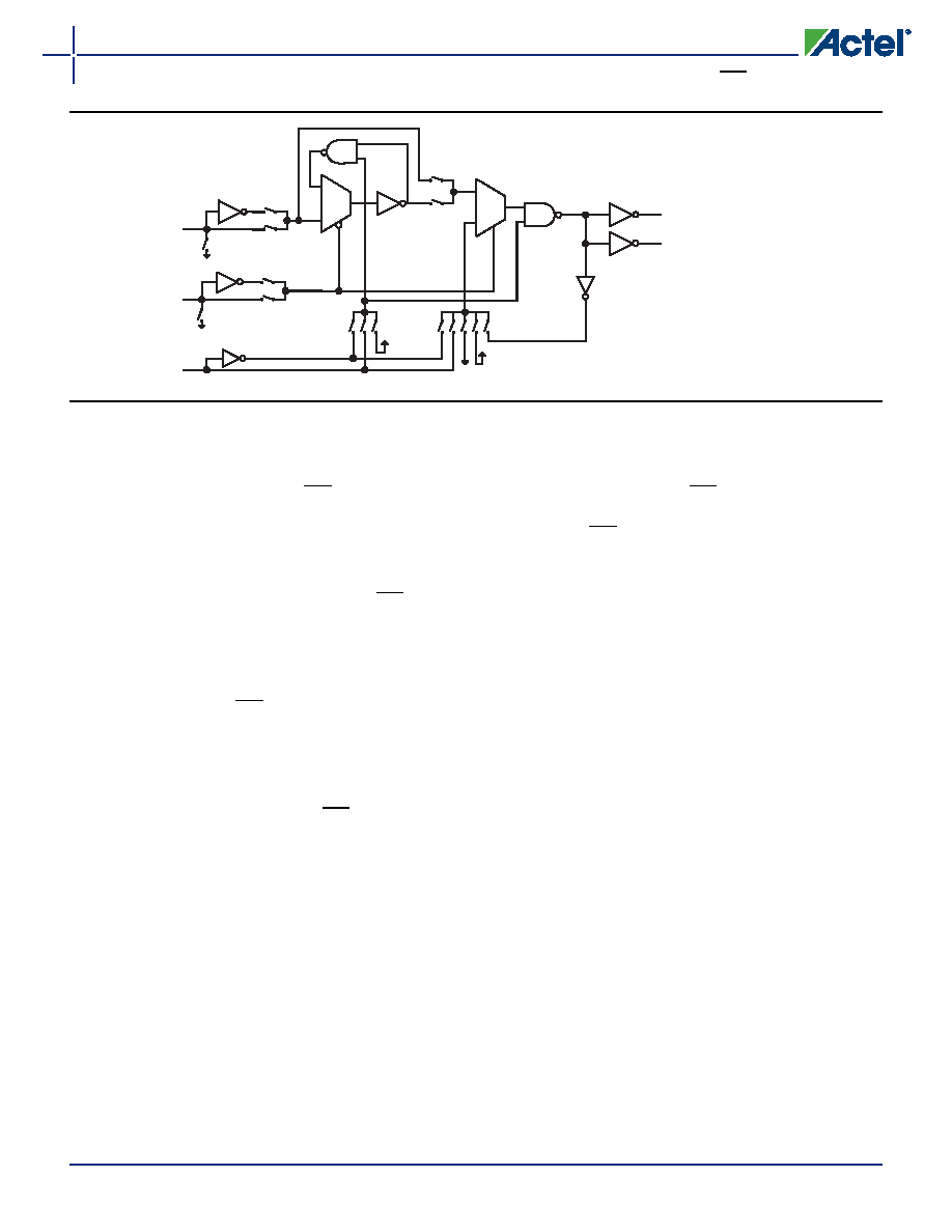
Logic Tile
The logic tile cell (Figure 1-3) has three inputs (any or all
of which can be inverted) and one output (which can
connect to both ultra-fast local and efficient long-line
routing resources). Any three-input, one-output logic
function (except a three-input XOR) can be configured as
one tile. The tile can be configured as a latch with clear
or set or as a flip-flop with clear or set. Thus, the tiles can
flexibly map logic and sequential gates of a design.
Figure 1-3 Core Logic Tile
Local Routing
In 1
In 2 (CLK)
In 3 (Reset)
Efficient Long-Line Routing
相關(guān)PDF資料 |
PDF描述 |
|---|---|
| ABB90DHRD | CONN CARD EXTEND 180POS .050" |
| ACB85DHLT | CONN EDGECARD 170PS .050 DIP SLD |
| EP2AGX65CU17C6N | IC ARRIA II GX FPGA 65K 358UBGA |
| IDT70V24L15PFG | IC SRAM 64KBIT 15NS 100TQFP |
| IDT71T75602S166PFG | IC SRAM 18MBIT 166MHZ 100TQFP |
相關(guān)代理商/技術(shù)參數(shù) |
參數(shù)描述 |
|---|---|
| APA600-FG896A | 制造商:ACTEL 制造商全稱:Actel Corporation 功能描述:Automotive-Grade ProASIC Flash Family FPGAs |
| APA600-FGB | 制造商:ACTEL 制造商全稱:Actel Corporation 功能描述:ProASIC Flash Family FPGAs |
| APA600-FGES | 制造商:ACTEL 制造商全稱:Actel Corporation 功能描述:ProASIC Flash Family FPGAs |
| APA600-FGG256 | 功能描述:IC FPGA PROASIC+ 600K 256-FBGA RoHS:是 類別:集成電路 (IC) >> 嵌入式 - FPGA(現(xiàn)場可編程門陣列) 系列:ProASICPLUS 產(chǎn)品培訓模塊:Three Reasons to Use FPGA's in Industrial Designs Cyclone IV FPGA Family Overview 特色產(chǎn)品:Cyclone? IV FPGAs 標準包裝:60 系列:CYCLONE® IV GX LAB/CLB數(shù):9360 邏輯元件/單元數(shù):149760 RAM 位總計:6635520 輸入/輸出數(shù):270 門數(shù):- 電源電壓:1.16 V ~ 1.24 V 安裝類型:表面貼裝 工作溫度:0°C ~ 85°C 封裝/外殼:484-BGA 供應(yīng)商設(shè)備封裝:484-FBGA(23x23) |
| APA600-FGG256A | 功能描述:IC FPGA PROASIC+ 600K 256-FBGA RoHS:是 類別:集成電路 (IC) >> 嵌入式 - FPGA(現(xiàn)場可編程門陣列) 系列:ProASICPLUS 產(chǎn)品培訓模塊:Three Reasons to Use FPGA's in Industrial Designs Cyclone IV FPGA Family Overview 特色產(chǎn)品:Cyclone? IV FPGAs 標準包裝:60 系列:CYCLONE® IV GX LAB/CLB數(shù):9360 邏輯元件/單元數(shù):149760 RAM 位總計:6635520 輸入/輸出數(shù):270 門數(shù):- 電源電壓:1.16 V ~ 1.24 V 安裝類型:表面貼裝 工作溫度:0°C ~ 85°C 封裝/外殼:484-BGA 供應(yīng)商設(shè)備封裝:484-FBGA(23x23) |
發(fā)布緊急采購,3分鐘左右您將得到回復(fù)。