- 您現(xiàn)在的位置:買賣IC網(wǎng) > PDF目錄375336 > AO8830 (ALPHA) Common-Drain Dual N-Channel Enhancement Mode Field Effect Transistor PDF資料下載
參數(shù)資料
| 型號: | AO8830 |
| 廠商: | ALPHA |
| 英文描述: | Common-Drain Dual N-Channel Enhancement Mode Field Effect Transistor |
| 中文描述: | 常見的漏雙N溝道增強型場效應(yīng)晶體管 |
| 文件頁數(shù): | 2/4頁 |
| 文件大?。?/td> | 122K |
| 代理商: | AO8830 |
AO8830
Symbol
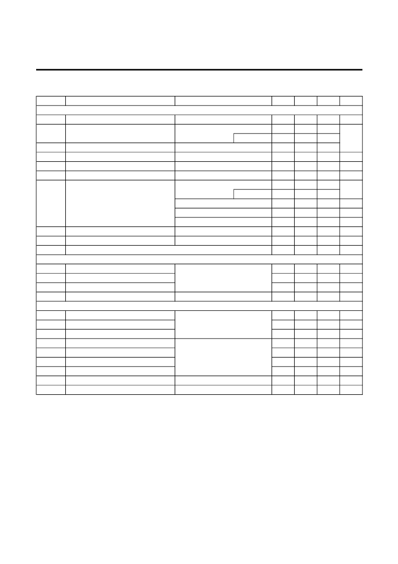
STATIC PARAMETERS
Min
Typ
Max
Units
BV
DSS
20
V
1
5
T
J
=55°C
I
GSS
BV
GSO
V
GS(th)
I
D(ON)
10
±12
0.5
30
V
V
A
0.6
1
22
31
25
32
42
21
0.75
27
T
J
=125°C
30
41
55
m
m
m
g
FS
V
SD
I
S
DYNAMIC PARAMETERS
Input Capacitance
Output Capacitance
S
V
A
1
2.5
C
iss
C
oss
C
rss
R
g
SWITCHING PARAMETERS
Total Gate Charge
Gate Source Charge
Gate Drain Charge
290
120
40
1.6
pF
pF
pF
k
Q
g
Q
gs
Q
gd
t
D(on)
t
r
t
D(off)
t
f
t
rr
Q
rr
5.2
2.1
1.9
280
972
2.35
2.2
nC
nC
nC
ns
ns
μ
s
μ
s
25
8
ns
nC
THIS PRODUCT HAS BEEN DESIGNED AND QUALIFIED FOR THE CONSUMER MARKET. APPLICATIONS OR USES AS CRITICAL
COMPONENTS IN LIFE SUPPORT DEVICES OR SYSTEMS ARE NOT AUTHORIZED. AOS DOES NOT ASSUME ANY LIABILITY ARISING
OUT OF SUCH APPLICATIONS OR USES OF ITS PRODUCTS. AOS RESERVES THE RIGHT TO IMPROVE PRODUCT DESIGN,
FUNCTIONS AND RELIABILITY WITHOUT NOTICE.
Body Diode Reverse Recovery Time
Body Diode Reverse Recovery Charge I
F
=6A, dI/dt=100A/
μ
s, V
GS
=-9V
Drain-Source Breakdown Voltage
On state drain current
I
D
=250
μ
A, V
GS
=0V
V
DS
=16V, V
GS
=0V
V
GS
=4.5V, V
DS
=5V
V
GS
=10V, I
D
=6A
Reverse Transfer Capacitance
Gate resistance
I
F
=6A, dI/dt=100A/
μ
s, V
GS
=-9V
μ
A
Electrical Characteristics (T
J
=25°C unless otherwise noted)
Parameter
Conditions
I
DSS
Zero Gate Voltage Drain Current
V
DS
=0V, V
GS
=±10V
V
DS
=0V, I
G
=±250uA
V
DS
=V
GS
I
D
=1mA
Gate-Body leakage current
Gate-Source Breakdown Voltage
Gate Threshold Voltage
R
DS(ON)
Static Drain-Source On-Resistance
Forward Transconductance
Diode Forward Voltage
m
V
GS
=2.5V, I
D
=4A
V
GS
=1.8V, I
D
=2A
I
S
=1A,V
GS
=0V
V
DS
=5V, I
D
=6A
V
GS
=4.5V, I
D
=5A
Turn-On Rise Time
Turn-Off DelayTime
Turn-Off Fall Time
V
GS
=4.5V, V
DS
=10V, R
L
=1.7
,
R
GEN
=3
V
GS
=0V, V
DS
=0V, f=1MHz
V
GS
=4.5V, V
DS
=10V, I
D
=6A
Turn-On DelayTime
V
GS
=0V, V
DS
=10V, f=1MHz
Maximum Body-Diode Continuous Current
A: The value of R
θ
JA
is measured with the device mounted on 1in
2
FR-4 board with 2oz. Copper, in a still air environment with T
A
=25°C. The
value in any given application depends on the user's specific board design. The currentand power rating is based on the t
≤
10s thermal
resistance rating.
B: Repetitive rating, pulse width limited by junction temperature.
C. The R
θ
JA
is the sum of the thermal impedence from junction to lead R
θ
JL
and lead to ambient.
D. The static characteristics in Figures 1 to 6,12,14 are obtained using 80
μ
s pulses, duty cycle 0.5% max.
E. These tests are performed with the device mounted on 1 in
curve provides a single pulse rating.
Rev 2: Aug 2006
2
FR-4 board with 2oz. Copper, in a still air environment with T
A
=25°C. The SOA
Alpha & Omega Semiconductor, Ltd.
相關(guān)PDF資料 |
PDF描述 |
|---|---|
| AO8846 | Common-Drain Dual N-Channel Enhancement Mode Field Effect Transistor |
| AO9926A | Circular Connector; No. of Contacts:8; Series:MS27656; Body Material:Aluminum; Connecting Termination:Crimp; Connector Shell Size:17; Circular Contact Gender:Pin; Circular Shell Style:Wall Mount Receptacle; Insert Arrangement:17-8 RoHS Compliant: No |
| AO9926B | Dual N-Channel Enhancement Mode Field Effect Transistor |
| AO9926BL | Dual N-Channel Enhancement Mode Field Effect Transistor |
| AO9926E | Dual N-Channel Enhancement Mode Field Effect Transistor |
相關(guān)代理商/技術(shù)參數(shù) |
參數(shù)描述 |
|---|---|
| AO8830_10 | 制造商:AOSMD 制造商全稱:Alpha & Omega Semiconductors 功能描述:Common-Drain Dual N-Channel Enhancement Mode Field Effect Transistor |
| AO8832 | 制造商:AOSMD 制造商全稱:Alpha & Omega Semiconductors 功能描述:Common-Drain Dual N-Channel Enhancement Mode Field Effect Transistor |
| AO8846 | 制造商:AOSMD 制造商全稱:Alpha & Omega Semiconductors 功能描述:Common-Drain Dual N-Channel Enhancement Mode Field Effect Transistor |
| AO9926 | 制造商:ALPHA 制造商全稱:ALPHA 功能描述:Dual N-Channel Enhancement Mode Field Effect Transistor |
| AO9926A | 制造商:AOSMD 制造商全稱:Alpha & Omega Semiconductors 功能描述:Dual N-Channel Enhancement Mode Field Effect Transistor |
發(fā)布緊急采購,3分鐘左右您將得到回復(fù)。