- 您現(xiàn)在的位置:買賣IC網(wǎng) > PDF目錄375308 > AM49PDL640AG70NT (SPANSION LLC) 64 Megabit (4 M x 16-Bit) CMOS 3.0 Volt-only, Simultaneous Operation Flash Memory and 16 Mbit (1 M x 16-Bit) Pseudo Static RAM PDF資料下載
參數(shù)資料
| 型號(hào): | AM49PDL640AG70NT |
| 廠商: | SPANSION LLC |
| 元件分類: | 存儲(chǔ)器 |
| 英文描述: | 64 Megabit (4 M x 16-Bit) CMOS 3.0 Volt-only, Simultaneous Operation Flash Memory and 16 Mbit (1 M x 16-Bit) Pseudo Static RAM |
| 中文描述: | SPECIALTY MEMORY CIRCUIT, PBGA73 |
| 封裝: | 13 X 9 MM, FBGA-73 |
| 文件頁(yè)數(shù): | 13/69頁(yè) |
| 文件大小: | 491K |
| 代理商: | AM49PDL640AG70NT |
第1頁(yè)第2頁(yè)第3頁(yè)第4頁(yè)第5頁(yè)第6頁(yè)第7頁(yè)第8頁(yè)第9頁(yè)第10頁(yè)第11頁(yè)第12頁(yè)當(dāng)前第13頁(yè)第14頁(yè)第15頁(yè)第16頁(yè)第17頁(yè)第18頁(yè)第19頁(yè)第20頁(yè)第21頁(yè)第22頁(yè)第23頁(yè)第24頁(yè)第25頁(yè)第26頁(yè)第27頁(yè)第28頁(yè)第29頁(yè)第30頁(yè)第31頁(yè)第32頁(yè)第33頁(yè)第34頁(yè)第35頁(yè)第36頁(yè)第37頁(yè)第38頁(yè)第39頁(yè)第40頁(yè)第41頁(yè)第42頁(yè)第43頁(yè)第44頁(yè)第45頁(yè)第46頁(yè)第47頁(yè)第48頁(yè)第49頁(yè)第50頁(yè)第51頁(yè)第52頁(yè)第53頁(yè)第54頁(yè)第55頁(yè)第56頁(yè)第57頁(yè)第58頁(yè)第59頁(yè)第60頁(yè)第61頁(yè)第62頁(yè)第63頁(yè)第64頁(yè)第65頁(yè)第66頁(yè)第67頁(yè)第68頁(yè)第69頁(yè)
November 20, 2003
Am49PDL640AG
11
P R E L I M I N A R Y
Requirements for Reading Array Data
To read array data from the outputs, the system must
drive the CE# and OE# pins to V
IL
. CE# is the power
control and selects the device. OE# is the output con-
trol and gates array data to the output pins. WE#
should remain at V
IH
.
The internal state machine is set for reading array data
upon device power-up, or after a hardware reset. This
ensures that no spurious alteration of the memory
content occurs during the power transition. No com-
mand is necessary in this mode to obtain array data.
Standard microprocessor read cycles that assert valid
addresses on the device address inputs produce valid
data on the device data outputs. Each bank remains
enabled for read access until the command register
contents are altered.
Refer to the AC Read-Only Operations table for timing
specifications and to Figure 14 for the timing diagram.
I
CC1
in the DC Characteristics table represents the ac-
tive current specification for reading array data.
Random Read (Non-Page Read)
Address access time (t
ACC
) is equal to the delay from
stable addresses to valid output data. The chip enable
access time (t
CE
) is the delay from the stable ad-
dresses and stable CE# to valid data at the output in-
puts. The output enable access time is the delay from
the falling edge of the OE# to valid data at the output
inputs (assuming the addresses have been stable for
at least t
ACC
–t
OE
time).
Page Mode Read
The device is capable of fast page mode read and is
compatible with the page mode Mask ROM read oper-
ation. This mode provides faster read access speed
for random locations within a page. The page size of
the device is 8 words, with the appropriate page being
selected by the higher address bits A21–A3 and the
LSB bits A2–A0 determining the specific word within
that page. This is an asynchronous operation with the
microprocessor supplying the specific word location.
The random or initial page access is equal to t
ACC
or
t
CE
and subsequent page read accesses (as long as
the locations specified by the microprocessor falls
within that page) is equivalent to t
PACC
. When CE# is
deasserted and reasserted for a subsequent access,
the access time is t
ACC
or t
CE
. Here again, CE# selects
the device and OE# is the output control and should
be used to gate data to the output inputs if the device
is selected. Fast page mode accesses are obtained by
keeping A21–A3 constant and changing A2 to A0 to
select the specific word within that page.
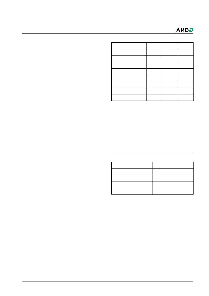
Table 2.
Page Select
Simultaneous Operation
The device is capable of reading data from one bank
of memory while a program or erase operation is in
progress in another bank of memory (simultaneous
operation), in addition to the conventional features
(read, program, erase-suspend read, and erase-sus-
pend program). The bank selected can be selected by
bank addresses (A21–A19) with zero latency.
The simultaneous operation can execute multi-func-
tion mode in the same bank.
Table 3.
Bank Select
Writing Commands/Command Sequences
To write a command or command sequence (which in-
cludes programming data to the device and erasing
sectors of memory), the system must drive WE# and
CE# to V
IL
, and OE# to V
IH
.
The device features an
Unlock Bypass
mode to facili-
tate faster programming. Once a bank enters the Un-
lock Bypass mode, only two write cycles are required
to program a word, instead of four. The “Word Pro-
gram Command Sequence” section has details on
programming data to the device using both standard
and Unlock Bypass command sequences.
An erase operation can erase one sector, multiple sec-
tors, or the entire device. Table 4 indicates the address
space that each sector occupies. A “bank address” is
the address bits required to uniquely select a bank.
Similarly, a “sector address” refers to the address bits
Word
A2
A1
A0
Word 0
0
0
0
Word 1
0
0
1
Word 2
0
1
0
Word 3
0
1
1
Word 4
1
0
0
Word 5
1
0
1
Word 6
1
1
0
Word 7
1
1
1
Bank
A21–A19
Bank A
000
Bank B
001, 010, 011
Bank C
100, 101, 110
Bank D
111
相關(guān)PDF資料 |
PDF描述 |
|---|---|
| AM49PDL640AG85NS | 64 Megabit (4 M x 16-Bit) CMOS 3.0 Volt-only, Simultaneous Operation Flash Memory and 16 Mbit (1 M x 16-Bit) Pseudo Static RAM |
| AM49PDL640AG85NT | 64 Megabit (4 M x 16-Bit) CMOS 3.0 Volt-only, Simultaneous Operation Flash Memory and 16 Mbit (1 M x 16-Bit) Pseudo Static RAM |
| AM49PDL640AGA70NS | 64 Megabit (4 M x 16-Bit) CMOS 3.0 Volt-only, Simultaneous Operation Flash Memory and 16 Mbit (1 M x 16-Bit) Pseudo Static RAM |
| AM49PDL640AGA70NT | 64 Megabit (4 M x 16-Bit) CMOS 3.0 Volt-only, Simultaneous Operation Flash Memory and 16 Mbit (1 M x 16-Bit) Pseudo Static RAM |
| AM50-0003 | LJT 128C 128#22D SKT WALL RECP |
相關(guān)代理商/技術(shù)參數(shù) |
參數(shù)描述 |
|---|---|
| AM49PDL640AG85NS | 制造商:SPANSION 制造商全稱:SPANSION 功能描述:64 Megabit (4 M x 16-Bit) CMOS 3.0 Volt-only, Simultaneous Operation Flash Memory and 16 Mbit (1 M x 16-Bit) Pseudo Static RAM |
| AM49PDL640AG85NT | 制造商:SPANSION 制造商全稱:SPANSION 功能描述:64 Megabit (4 M x 16-Bit) CMOS 3.0 Volt-only, Simultaneous Operation Flash Memory and 16 Mbit (1 M x 16-Bit) Pseudo Static RAM |
| AM49PDL640AGA70NS | 制造商:SPANSION 制造商全稱:SPANSION 功能描述:64 Megabit (4 M x 16-Bit) CMOS 3.0 Volt-only, Simultaneous Operation Flash Memory and 16 Mbit (1 M x 16-Bit) Pseudo Static RAM |
| AM49PDL640AGA70NT | 制造商:SPANSION 制造商全稱:SPANSION 功能描述:64 Megabit (4 M x 16-Bit) CMOS 3.0 Volt-only, Simultaneous Operation Flash Memory and 16 Mbit (1 M x 16-Bit) Pseudo Static RAM |
| AM4-A2-A-30-3 | 制造商:HEINEMANN / EATON 功能描述: |
發(fā)布緊急采購(gòu),3分鐘左右您將得到回復(fù)。