- 您現(xiàn)在的位置:買賣IC網(wǎng) > PDF目錄375306 > AM42BDS640AGTD8IT (SPANSION LLC) Circular Connector; No. of Contacts:13; Series:MS27468; Body Material:Aluminum; Connecting Termination:Crimp; Connector Shell Size:11; Circular Contact Gender:Socket; Circular Shell Style:Jam Nut Receptacle; Insert Arrangement:11-35 RoHS Compliant: No PDF資料下載
參數(shù)資料
| 型號: | AM42BDS640AGTD8IT |
| 廠商: | SPANSION LLC |
| 元件分類: | 存儲器 |
| 英文描述: | Circular Connector; No. of Contacts:13; Series:MS27468; Body Material:Aluminum; Connecting Termination:Crimp; Connector Shell Size:11; Circular Contact Gender:Socket; Circular Shell Style:Jam Nut Receptacle; Insert Arrangement:11-35 RoHS Compliant: No |
| 中文描述: | SPECIALTY MEMORY CIRCUIT, PBGA93 |
| 封裝: | 8 X 11.60 MM, FBGA-93 |
| 文件頁數(shù): | 28/72頁 |
| 文件大?。?/td> | 1060K |
| 代理商: | AM42BDS640AGTD8IT |
第1頁第2頁第3頁第4頁第5頁第6頁第7頁第8頁第9頁第10頁第11頁第12頁第13頁第14頁第15頁第16頁第17頁第18頁第19頁第20頁第21頁第22頁第23頁第24頁第25頁第26頁第27頁當前第28頁第29頁第30頁第31頁第32頁第33頁第34頁第35頁第36頁第37頁第38頁第39頁第40頁第41頁第42頁第43頁第44頁第45頁第46頁第47頁第48頁第49頁第50頁第51頁第52頁第53頁第54頁第55頁第56頁第57頁第58頁第59頁第60頁第61頁第62頁第63頁第64頁第65頁第66頁第67頁第68頁第69頁第70頁第71頁第72頁
November 1, 2002
Am42BDS640AG
27
P R E L I M I N A R Y
Unlock Bypass Command Sequence
The unlock bypass feature allows the system to prima-
rily program to a bank faster than using the standard
program command sequence. The unlock bypass
command sequence is initiated by first writing two
unlock cycles. This is followed by a third write cycle
containing the unlock bypass command, 20h. That
bank then enters the unlock bypass mode. A two-cycle
unlock bypass program command sequence is all that
is required to program in this mode. The first cycle in
this sequence contains the unlock bypass program
command, A0h; the second cycle contains the program
address and data. Additional data is programmed in
the same manner. This mode dispenses with the initial
two unlock cycles required in the standard program
command sequence, resulting in faster total program-
ming time. The host system may also initiate the chip
erase and sector erase sequences in the unlock
bypass mode. The erase command sequences are
four cycles in length instead of six cycles.
Table 14,
“Command Definitions,” on page 30
shows the require-
ments for the unlock bypass command sequences.
During the unlock bypass mode, only the Unlock
Bypass Program, Unlock Bypass Sector Erase, Unlock
Bypass Chip Erase, and Unlock Bypass Reset com-
mands are valid. To exit the unlock bypass mode, the
system must issue the two-cycle unlock bypass reset
command sequence. The first cycle must contain the
bank address and the data 90h. The second cycle
need only contain the data 00h. The bank then returns
to the read mode.
The device offers accelerated program operations
through the ACC input. When the system asserts V
ID
on this input, the device automatically enters the
Unlock Bypass mode. The system may then write the
two-cycle Unlock Bypass program command
sequence. The device uses the higher voltage on the
ACC input to accelerate the operation.
Figure 2
illustrates the algorithm for the program oper-
ation. Refer to the Erase/Program Operations table in
the AC Characteristics section for parameters, and
Figure 21, “Asynchronous Program Operation Tim-
ings,” on page 51
for timing diagrams.
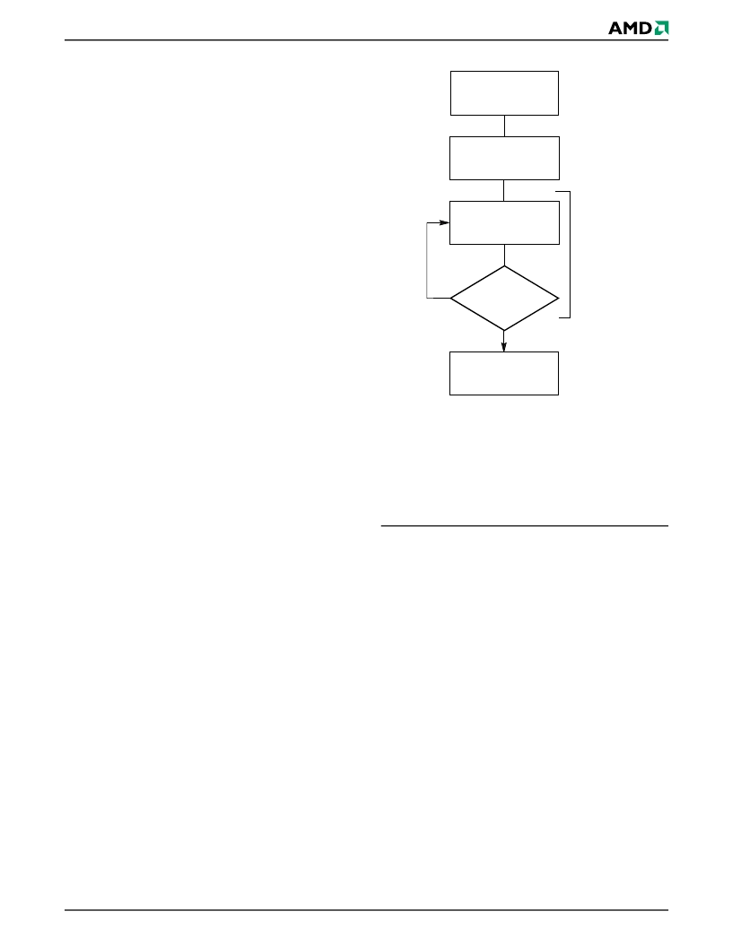
Figure 2.
Erase Operation
Chip Erase Command Sequence
Chip erase is a six bus cycle operation. The chip erase
command sequence is initiated by writing two unlock
cycles, followed by a set-up command. Two additional
unlock write cycles are then followed by the chip erase
command, which in turn invokes the Embedded Erase
algorithm. The device does not require the system to
preprogram prior to erase. The Embedded Erase algo-
rithm automatically preprograms and verifies the entire
memory for an all zero data pattern prior to electrical
erase. The system is not required to provide any con-
trols or timings during these operations.
Table 14,
“Command Definitions,” on page 30
shows the address
and data requirements for the chip erase command
sequence.
When the Embedded Erase algorithm is complete, that
bank returns to the read mode and addresses are no
longer latched. The system can determine the status of
the erase operation by using DQ7 or DQ6/DQ2. Refer
to the
“Flash Write Operation Status” section on page
31
section for information on these status bits.
START
Write Erase
Command Sequence
Data Poll
from System
Data = FFh
No
Yes
Erasure Completed
Embedded
Erase
algorithm
in progress
Notes:
1. See Table 14 for erase command sequence.
2. See the section on DQ3 for information on the sector
erase timer.
相關(guān)PDF資料 |
PDF描述 |
|---|---|
| AM42BDS640AGBD8IS | RES 93.1K-OHM 0.1% 0.125W 50PPM THIN-FILM SMD-1206 TR-7-PL ROHS |
| AM42BDS640AGBD8IT | Stacked Multi-Chip Package (MCP) Flash Memory and SRAM |
| AM42BDS640AGTD9IS | LJT 13C 13#22D SKT WALL RECP |
| AM42BDS640AGTD9IT | Stacked Multi-Chip Package (MCP) Flash Memory and SRAM |
| AM42DL1624DB70IT | Stacked Multi-Chip Package (MCP) Flash Memory and SRAM |
相關(guān)代理商/技術(shù)參數(shù) |
參數(shù)描述 |
|---|---|
| AM42BDS640AGTD9IS | 制造商:AMD 制造商全稱:Advanced Micro Devices 功能描述:64 Megabit (4 M x 16-Bit) CMOS 1.8 Volt-only, Simultaneous Operation, Burst Mode Flash Memory and 16 Mbit (1 M x 16-Bit) Static RAM |
| AM42BDS640AGTD9IT | 制造商:AMD 制造商全稱:Advanced Micro Devices 功能描述:64 Megabit (4 M x 16-Bit) CMOS 1.8 Volt-only, Simultaneous Operation, Burst Mode Flash Memory and 16 Mbit (1 M x 16-Bit) Static RAM |
| AM42DL1612DB30IS | 制造商:AMD 制造商全稱:Advanced Micro Devices 功能描述:Am29DL16xD 16 Megabit (2 M x 8-Bit/1 M x 16-Bit) CMOS 3.0 Volt-only, Simultaneous Operation Flash Memory and 2 Mbit (128 K x 16-Bit) Static RAM |
| AM42DL1612DB30IT | 制造商:AMD 制造商全稱:Advanced Micro Devices 功能描述:Am29DL16xD 16 Megabit (2 M x 8-Bit/1 M x 16-Bit) CMOS 3.0 Volt-only, Simultaneous Operation Flash Memory and 2 Mbit (128 K x 16-Bit) Static RAM |
| AM42DL1612DB35IS | 制造商:AMD 制造商全稱:Advanced Micro Devices 功能描述:Am29DL16xD 16 Megabit (2 M x 8-Bit/1 M x 16-Bit) CMOS 3.0 Volt-only, Simultaneous Operation Flash Memory and 2 Mbit (128 K x 16-Bit) Static RAM |
發(fā)布緊急采購,3分鐘左右您將得到回復(fù)。