- 您現(xiàn)在的位置:買賣IC網(wǎng) > PDF目錄57790 > AH312-S8G (TRIQUINT SEMICONDUCTOR INC) 400 MHz - 2300 MHz RF/MICROWAVE WIDE BAND MEDIUM POWER AMPLIFIER PDF資料下載
參數(shù)資料
| 型號: | AH312-S8G |
| 廠商: | TRIQUINT SEMICONDUCTOR INC |
| 元件分類: | 放大器 |
| 英文描述: | 400 MHz - 2300 MHz RF/MICROWAVE WIDE BAND MEDIUM POWER AMPLIFIER |
| 封裝: | GREEN, MS-012, SMT, SOIC-8 |
| 文件頁數(shù): | 1/7頁 |
| 文件大小: | 356K |
| 代理商: | AH312-S8G |
Specifications and information are subject to change without notice.
WJ Communications, Inc
Phone 1-800-WJ1-4401 FAX: 408-577-6621 e-mail: sales@wj.com Web site: www.wj.com
Page 1 of 7 March 2006
AH312
2 Watt, High Linearity InGaP HBT Amplifier
Product Information
The Communications Edge
TM
Product Features
400 – 2300 MHz
+33 dBm P1dB
+51 dBm Output IP3
18 dB Gain @ 900 MHz
+5V Single Positive Supply
MTTF > 100 Years
Lead-free/green/RoHS-compliant
SOIC-8 SMT Pkg.
Applications
Final stage amplifiers for Repeaters
Mobile Infrastructure
Product Description
The AH312 is a high dynamic range driver amplifier in a
low-cost surface mount package. The InGaP/GaAs HBT is
able to achieve high performance for various narrowband-
tuned application circuits with up to +49 dBm OIP3 and
+33 dBm of compressed 1dB power. It is housed in a lead-
free/green/RoHS-compliant SOIC-8 package. All devices are
100% RF and DC tested.
The AH312 is targeted for use as a driver amplifier in
wireless infrastructure where high linearity and medium
power is required.
An internal active bias allows the
AH312 to maintain high linearity over temperature and
operate directly off a single +5V supply. This combination
makes the device an excellent candidate for transceiver line
cards in current and next generation multi-carrier 3G base
stations.
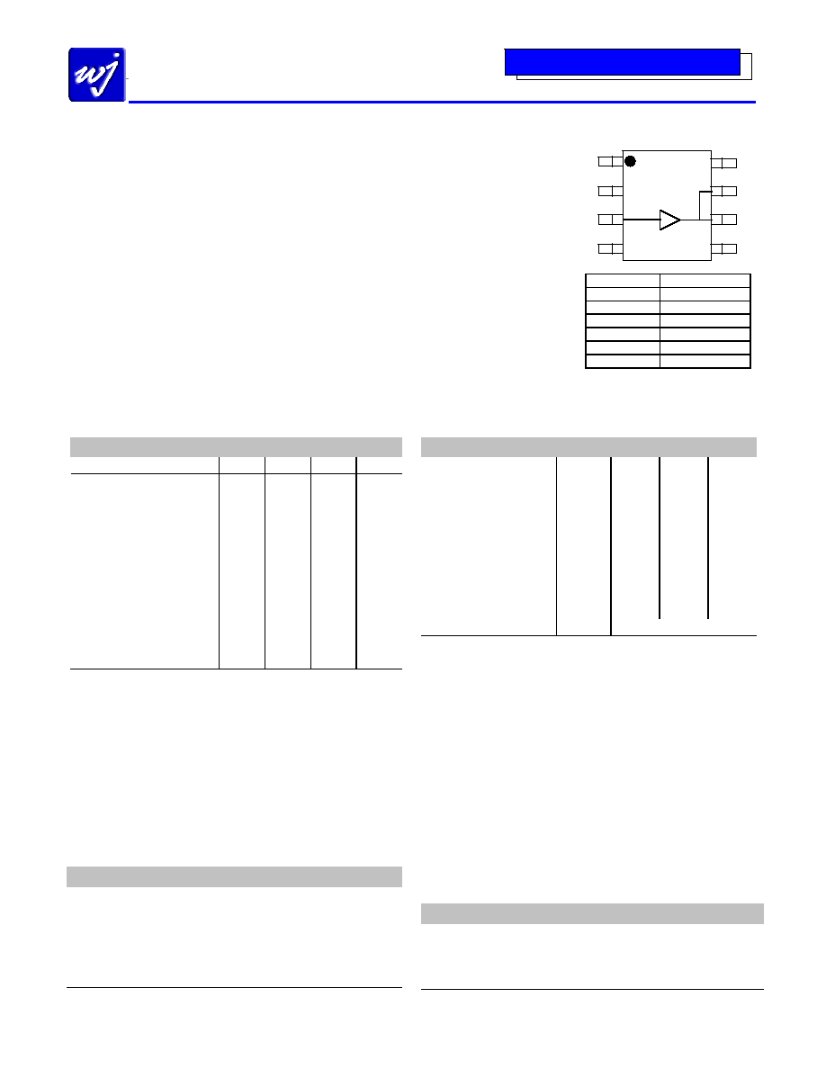
Functional Diagram
Function
Pin No.
Vref
1
Input
3
Output
6, 7
Vbias
8
GND
Backside Paddle
N/C or GND
2, 4, 5
Specifications
(1)
Parameter
Units
Min
Typ
Max
Operational Bandwidth
MHz
400
2300
Test Frequency
MHz
2140
Gain
dB
9
10
Input R.L.
dB
20
Output R.L.
dB
6.8
Output P1dB
dBm
+32
+33.2
Output IP3
(2)
dBm
+47
+48
IS-95A Channel Power
@ -45 dBc ACPR, 1960 MHz
dBm
+27.5
wCDMA Channel Power
@ -45 dBc ACLR, 2140 MHz
dBm
+25.3
Noise Figure
dB
7.7
Operating Current Range, Icc
(3)
mA
700
800
900
Device Voltage, Vcc
V
+5
1. Test conditions unless otherwise noted: 25C, +5V Vsupply, 2140 MHz, in tuned application circuit.
2. 3OIP measured with two tones at an output power of +17 dBm/tone separated by 1 MHz. The
suppression on the largest IM3 product is used to calculate the 3OIP using a 2:1 rule.
3. This corresponds to the quiescent current or operating current under small-signal conditions into
pins 6, 7, and 8. It is expected that the current can increase by an additional 200 mA at P1dB. Pin
1 is used as a reference voltage for the internal biasing circuitry. It is expected that Pin 1 will pull
22mA of current when used with a series bias resistor of R1=15
Ω. (ie. total device current
typically will be 822 mA.)
Absolute Maximum Rating
Parameter
Rating
Operating Case Temperature
-40 to +85
°C
Storage Temperature
-65 to +150
°C
RF Input Power (continuous)
+28 dBm
Device Voltage
+8 V
Device Current
1400 mA
Device Power
8 W
Junction Temperature
+250
°C
Operation of this device above any of these parameters may cause permanent damage.
Typical Performance
(4)
Parameter
Units
Typical
Frequency
MHz
900
1960
2140
S21 – Gain
dB
18
11
10
S11 – Input R.L.
dB
-18
-19
-20
S22 – Output R.L.
dB
-11
-6.8
Output P1dB
dBm
+33
+33.4
+33.2
Output IP3
dBm
+49
+51
+48
IS-95A Channel Power
@ -45 dBc ACPR
dBm
+27
+27.5
wCDMA Channel Power
@ -45 dBc ACLR
dBm
+25.3
Noise Figure
dB
8.0
7.3
7.7
Device Bias
(3)
+5 V @ 800 mA
4. Typical parameters reflect performance in a tuned application circuit at +25
° C.
Ordering Information
Part No.
Description
AH312-S8G
2 Watt, High Linearity InGaP HBT Amplifier
(lead-free/green/RoHS-compliant SOIC-8 Pkg)
AH312-S8PCB900
900 MHz Evaluation Board
AH312-S8PCB1960
1960 MHz Evaluation Board
AH312-S8PCB2140
2140 MHz Evaluation Board
1
2
3
4
8
7
6
5
相關(guān)PDF資料 |
PDF描述 |
|---|---|
| AH337-PL | MAGNETIC FIELD SENSOR-HALL EFFECT |
| AH373-WLA | MAGNETIC FIELD SENSOR-HALL EFFECT, -6-6mT, 0.30-0.40V, RECTANGULAR, SURFACE MOUNT |
| AH373-WL-A | MAGNETIC FIELD SENSOR-HALL EFFECT, -6-6mT, 0.30-0.40V, RECTANGULAR, SURFACE MOUNT |
| AH373-WG-A | MAGNETIC FIELD SENSOR-HALL EFFECT, -6-6mT, 0.30-0.40V, RECTANGULAR, SURFACE MOUNT |
| AH477AZ4-AG1 | MAGNETIC FIELD SENSOR-HALL EFFECT, -7-7mT, RECTANGULAR, THROUGH HOLE MOUNT |
相關(guān)代理商/技術(shù)參數(shù) |
參數(shù)描述 |
|---|---|
| AH312-S8PCB1960 | 功能描述:射頻開發(fā)工具 1960MHz Eval Brd 11dB Gain RoHS:否 制造商:Taiyo Yuden 產(chǎn)品:Wireless Modules 類型:Wireless Audio 工具用于評估:WYSAAVDX7 頻率: 工作電源電壓:3.4 V to 5.5 V |
| AH312-S8PCB2140 | 功能描述:射頻開發(fā)工具 2140MHz Eval Brd 10dB Gain RoHS:否 制造商:Taiyo Yuden 產(chǎn)品:Wireless Modules 類型:Wireless Audio 工具用于評估:WYSAAVDX7 頻率: 工作電源電壓:3.4 V to 5.5 V |
| AH312-S8PCB900 | 功能描述:射頻開發(fā)工具 900MHz Eval Brd 18dB Gain RoHS:否 制造商:Taiyo Yuden 產(chǎn)品:Wireless Modules 類型:Wireless Audio 工具用于評估:WYSAAVDX7 頻率: 工作電源電壓:3.4 V to 5.5 V |
| AH312-S8TRG | 制造商:TriQuint Semiconductor 功能描述:RF & MW POWER AMPLIFIER |
| AH314 | 制造商:TriQuint Semiconductor 功能描述:RF & MW DRIVER AMPLIFIER |
發(fā)布緊急采購,3分鐘左右您將得到回復。