- 您現(xiàn)在的位置:買賣IC網(wǎng) > PDF目錄374037 > ADSP-21XX4444 (Analog Devices, Inc.) ADSP-2100 Family DSP Microcomputers PDF資料下載
參數(shù)資料
| 型號(hào): | ADSP-21XX4444 |
| 廠商: | Analog Devices, Inc. |
| 英文描述: | ADSP-2100 Family DSP Microcomputers |
| 中文描述: | 的ADSP - 2100系列DSP的微機(jī) |
| 文件頁(yè)數(shù): | 17/32頁(yè) |
| 文件大小: | 231K |
| 代理商: | ADSP-21XX4444 |
第1頁(yè)第2頁(yè)第3頁(yè)第4頁(yè)第5頁(yè)第6頁(yè)第7頁(yè)第8頁(yè)第9頁(yè)第10頁(yè)第11頁(yè)第12頁(yè)第13頁(yè)第14頁(yè)第15頁(yè)第16頁(yè)當(dāng)前第17頁(yè)第18頁(yè)第19頁(yè)第20頁(yè)第21頁(yè)第22頁(yè)第23頁(yè)第24頁(yè)第25頁(yè)第26頁(yè)第27頁(yè)第28頁(yè)第29頁(yè)第30頁(yè)第31頁(yè)第32頁(yè)
ADSP-21mod870
–17–
REV. 0
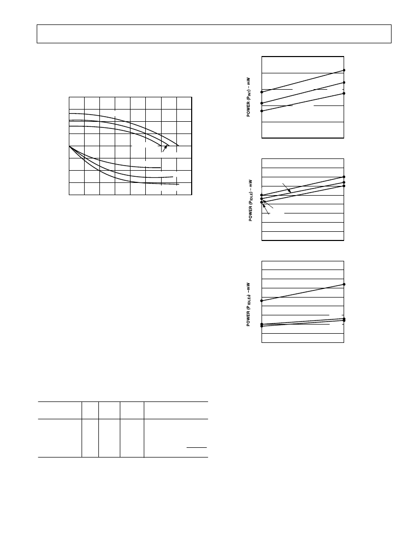
OUTPUT DRIVE CURRENTS
Figure 14 shows typical I-V characteristics for the output driv-
ers of the ADSP-21mod870. The curves represent the current
drive capability of the output drivers as a function of output
voltage.
SOURCE VOLTAGE – V
80
–40
0
4.0
S
0.5
1.0
1.5
2.0
3.0
3.5
60
–20
–60
–80
40
0
20
3.0V, +85
°
C
3.3V, +25
°
C
3.6V, –40
°
C
3.0V, +85
°
C
3.3V, +25
°
C
3.6V, –40
°
C
2.5
Figure 14. Typical Drive Currents
POWER DISSIPATION
To determine total power dissipation in a specific application,
the following equation should be applied for each output:
C
×
V
×
f
C
= load capacitance,
f
= output switching frequency.
Example
In an application where external data memory is used and no
other outputs are active, power dissipation is calculated as follows:
Assumptions
External data memory is accessed every cycle with 50% of
the address pins switching.
External data memory writes occur every other cycle with
50% of the data pins switching.
Each address and data pin has a 10 pF total load at the pin.
The application operates at V
DD
= 3.3 V and t
CK
= 30 ns.
Total Power Dissipation = P
INT
+ (
C
×
V
DD
2
×
f
)
P
INT
= internal power dissipation from Power vs. Frequency
graph (Figure 15).
(
C
×
V
DD
2
×
f
) is calculated for each output:
# of
Pins
3
C
3
V
DD2
3
f
Address,
DMS
Data Output,
WR
9
RD
CLKOUT
8
×
10 pF
×
10 pF
×
10 pF
×
10 pF
×
3.3
2
V
×
3.3
2
V
×
3.3
2
V
×
3.3
2
V
×
33.3
2
MHz = 29.0 mW
×
16.67 MHz = 16.3 mW
×
16.67 MHz = 1.8 mW
×
33.3 MHz =
1
1
3.6 mW
50.7 mW
Total power dissipation for this example is P
INT
+ 50.7 mW.
1/t
CK
– MHz
250
150
33.3
52
100
200
50
0
21mod870 POWER, INTERNAL
1, 3, 4
V
DD
= 3.6V
V
DD
= 3.3V
V
DD
= 3.0V
216mW
168.3mW
132mW
144mW
112.2mW
87mW
1/f
CK
– MHz
45
25
10
33.3
52
40
20
15
35
30
5
0
POWER, IDLE
1, 2, 3
V
DD
= 3.6V
V
DD
= 3.3V
V
DD
= 3.0V
35mW
30mW
25mW
23mW
21mW
1/f
CK
– MHz
45
15
33.3
25
20
35
30
10
5
0
POWER, IDLE nMODES
3
52
IDLE
IDLE (16)
IDLE (128)
13mW
12mW
23mW
10mW
9mW
VALID FOR ALL TEMPERATURE GRADES.
1
POWER REFLECTS DEVICE OPERATING WITH NO OUTPUT LOADS.
2
IDLE REFERS TO ADSP-21mod870 STATE OF OPERATION DURING EXECUTION OF
IDLE INSTRUCTION. DEASSERTED PINS ARE DRIVEN TO EITHER V
DD
OR GND.
3
TYPICAL POWER DISSIPATION AT 3.3V V
DD
AND +25
8
C, EXCEPT WHERE SPECIFIED.
4
I
DD
MEASUREMENT TAKEN WITH ALL INSTRUCTIONS EXECUTING FROM INTERNAL
MEMORY. 50% OF THE INSTRUCTIONS ARE MULTIFUNCTION (TYPES 1, 4, 5, 12, 13, 14),
30% ARE TYPE 2 AND TYPE 6, AND 20% ARE IDLE INSTRUCTIONS.
40
32mW
32mW
Figure 15. Power vs. Frequency
相關(guān)PDF資料 |
PDF描述 |
|---|---|
| ADSP-21MSP5859 | LM101A/LM201A/LM301A Operational Amplifiers; Package: MDIP; No of Pins: 8; Qty per Container: 40; Container: Rail |
| ADSP-21XX | ADSP-2100 Family DSP Microcomputers |
| ADSP-21MOD970-110 | Multiport Internet Gateway Processor Solution |
| ADSP-21mod970-110 | Data Pump Solution Gateway Processor Solution(多端口網(wǎng)關(guān)處理器解決方案) |
| ADSP-21MOD980N | MultiPort Internet Gateway Processor |
相關(guān)代理商/技術(shù)參數(shù) |
參數(shù)描述 |
|---|---|
| ADSP-3128AJG | 制造商:Rochester Electronics LLC 功能描述:- Bulk 制造商:Analog Devices 功能描述: |
| ADSP-3128ASG/883B | 制造商:Rochester Electronics LLC 功能描述:- Bulk |
| ADSP-3201JG | 制造商:Rochester Electronics LLC 功能描述:- Bulk 制造商:Analog Devices 功能描述: |
| ADSP-3201KG | 制造商:Rochester Electronics LLC 功能描述:- Bulk 制造商:Analog Devices 功能描述:MULTIPLIER, 144 Pin, Ceramic, PGA |
| ADSP-3201TG | 制造商:Rochester Electronics LLC 功能描述:- Bulk |
發(fā)布緊急采購(gòu),3分鐘左右您將得到回復(fù)。