- 您現(xiàn)在的位置:買賣IC網(wǎng) > PDF目錄374037 > ADSP-21MOD980N (Analog Devices, Inc.) MultiPort Internet Gateway Processor PDF資料下載
參數(shù)資料
| 型號(hào): | ADSP-21MOD980N |
| 廠商: | Analog Devices, Inc. |
| 英文描述: | MultiPort Internet Gateway Processor |
| 中文描述: | 通寶互聯(lián)網(wǎng)網(wǎng)關(guān)處理器 |
| 文件頁數(shù): | 13/42頁 |
| 文件大小: | 566K |
| 代理商: | ADSP-21MOD980N |
第1頁第2頁第3頁第4頁第5頁第6頁第7頁第8頁第9頁第10頁第11頁第12頁當(dāng)前第13頁第14頁第15頁第16頁第17頁第18頁第19頁第20頁第21頁第22頁第23頁第24頁第25頁第26頁第27頁第28頁第29頁第30頁第31頁第32頁第33頁第34頁第35頁第36頁第37頁第38頁第39頁第40頁第41頁第42頁
13
REV. PrB
6/2001
For current information contact Analog Devices at (800) ANALOGD
ADSP-21mod980N
PRELIMINARY TECHNICAL DATA
ever, to write to the processor
’
s memory-mapped control
registers. A typical IDMA transfer process is described as
follows:
1.
Host starts IDMA transfer
2.
Host uses IS and IAL control lines to latch either the
DMA starting address (IDMAA) or the PM/DM
OVLAY selection into the processor
’
s IDMA control
registers.
If IAD [15] = 1, the value of IAD [7:0] represents the
IDMA overlay: IAD[14:8] must be set to 0.
If IAD [15] = 0, the value of IAD [13:0] represents the
starting address of internal memory to be accessed and
IAD [14] reflects PM or DM for access.
1.
Host uses IS and IRD (or IWR) to read (or write) pro-
cessor internal memory (PM or DM).
2.
Host ends IDMA transfer.
The IDMA port has a 16-bit multiplexed address and data
bus and supports 24-bit program memory. The IDMA port
is completely asynchronous and can be written to, while the
ADSP-21mod980N is operating at full speed.
The processor memory address is latched and then auto-
matically incremented after each IDMA transaction. An
external device can therefore access a block of sequentially
addressed memory by specifying only the starting address of
the block. This increases throughput as the address does
not have to be sent for each memory access.
IDMA Port access occurs in two phases. The first is the
IDMA Address Latch cycle
. When the acknowledge is
asserted, a 14-bit address and 1-bit destination type can be
driven onto the bus by an external device. The address
specifies an on-chip memory location, the destination type
specifies whether it is a DM or PM access. The falling edge
of the address latch signal latches this value into the
IDMAA register.
Once the address is stored, data can then be either read
from, or written to, the ADSP-21mod980N
’
s on-chip
memory. Asserting the select line (IS) and the appropriate
read or write line (IRD and IWR respectively) signals the
ADSP-21mod980N that a particular transaction is
required. In either case, there is a one-processor-cycle delay
for synchronization. The memory access consumes one
additional processor cycle.
Once an access has occurred, the latched address is auto-
matically incremented, and another access can occur.
Through the IDMAA register, the processor can also spec-
ify the starting address and data format for DMA operation.
Asserting the IDMA port select (IS) and address latch
enable (IAL) directs the ADSP-21mod980N to write the
address onto the IAD [14:0] bus into the IDMA Control
Register. If IAD [15] is set to 0, IDMA latches the address.
If IAD [15] is set to 1, IDMA latches OVLAY memory. The
IDMAA register is memory mapped at address DM
(0x3FE0). Note that the latched address (IDMAA) or over-
lay register cannot be read back by the host. The IDMA
OVERLAY register is memory mapped at address
DM(0x3FE7). See
Figure on page 13
for more informa-
tion on IDMA memory mapping. When bit 14 in 0x3FE7
is set to 1, then timing in
Figure on page 35
applies for
short reads. When bit 14 in 0x3FE7 is set to zero short
reads use the timing shown in
Figure on page 34
.
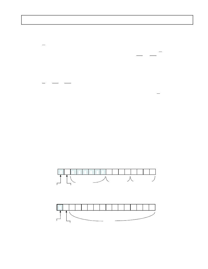
Figure 9. IDMA Control/OVLAY Registers
15
14
13
12
11
10
9
8
7
6
5
4
3
2
1
0
IDMA OVERLAY
DM(0x3FE7)
ID DMOVLAY
ID PMOVLAY
RESERVED
SET TO 0
15
14
13
12
11
10
9
8
7
6
5
4
3
2
1
0
IDMA CONTROL (U=UNDEFINED AT RESET)
U
DM(0x3FE0)
IDMAA
ADDRESS
IDMAD
Destination memory type:
0=PM
1=DM
U
U
U
U
U
U
U
U
U
U
U
U
U
U
Short Read Only
Enable
1 = Enable
0 = Disable
0
0
0
0
0
0
0
0
0
0
0
0
0
0
0
0
0
RESERVED
ALWAYS SET
TO 0
RESERVED
ALWAYS SET
TO 0
相關(guān)PDF資料 |
PDF描述 |
|---|---|
| ADSP-21MOD980N-000 | CAP 27PF 100V 10% X7R AXIAL BULK M-MIL-PRF-39014 |
| ADSP-21MSP58BST-104 | DSP Microcomputers |
| ADSP-BF531 | Blackfin Embedded Processor |
| ADSP-BF531SBBC400 | Metal Connector Backshell |
| ADSP-BF531SBBZ400 | Blackfin Embedded Processor |
相關(guān)代理商/技術(shù)參數(shù) |
參數(shù)描述 |
|---|---|
| ADSP-21MSP50ABG-52 | 制造商:Analog Devices 功能描述: |
| adsp-21msp50akg-52 | 制造商:Rochester Electronics LLC 功能描述:- Bulk 制造商:Analog Devices 功能描述: |
| ADSP-21MSP50BG-52 | 制造商:Rochester Electronics LLC 功能描述:- Bulk |
| ADSP-21MSP50KG-52 | 制造商:Rochester Electronics LLC 功能描述:- Bulk |
| ADSP-21MSP52-520010 | 制造商:Analog Devices 功能描述: |
發(fā)布緊急采購(gòu),3分鐘左右您將得到回復(fù)。