- 您現(xiàn)在的位置:買賣IC網(wǎng) > PDF目錄375264 > ADS7819U 12-Bit 800kHz Sampling CMOS ANALOG-to-DIGITAL CONVERTER PDF資料下載
參數(shù)資料
| 型號(hào): | ADS7819U |
| 英文描述: | 12-Bit 800kHz Sampling CMOS ANALOG-to-DIGITAL CONVERTER |
| 中文描述: | 12位800kHz采樣CMOS模擬數(shù)字轉(zhuǎn)換器 |
| 文件頁(yè)數(shù): | 2/11頁(yè) |
| 文件大?。?/td> | 317K |
| 代理商: | ADS7819U |
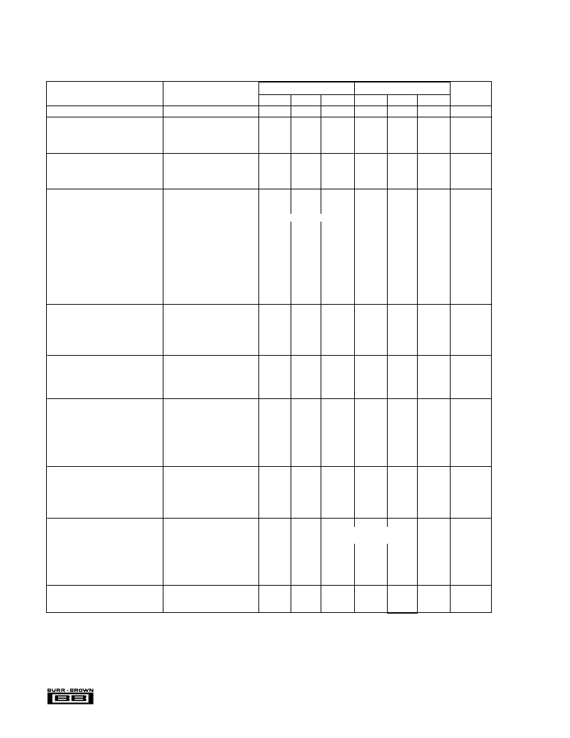
2
ADS7819
SPECIFICATIONS
At T
A
= –40
°
C to +85
°
C, f
S
= 800kHz, +V
DIG
= +V
ANA
= +5V, –V
ANA
= –5V, using internal reference and the 50
input resistor shown in Figure 4b, unless otherwise specified.
The information provided herein is believed to be reliable; however, BURR-BROWN assumes no responsibility for inaccuracies or omissions. BURR-BROWN assumes
no responsibility for the use of this information, and all use of such information shall be entirely at the user’s own risk. Prices and specifications are subject to change
without notice. No patent rights or licenses to any of the circuits described herein are implied or granted to any third party. BURR-BROWN does not authorize or warrant
any BURR-BROWN product for use in life support devices and/or systems.
ADS7819P, U
ADS7819PB, UB
PARAMETER
CONDITIONS
MIN
TYP
MAX
MIN
TYP
MAX
UNITS
RESOLUTION
12
*
Bits
ANALOG INPUT
Voltage Range
Impedance
Capacitance
±
2.5
3.1
5
*
*
*
V
k
pF
THROUGHPUT SPEED
Conversion Time
Complete Cycle
Throughput Rate
940
*
ns
ns
kHz
Acquire & Convert
1250
*
800
*
DC ACCURACY
Integral Linearity Error
Differential Linearity Error
No Missing Codes
Transition Noise
(2)
Full Scale Error
(3, 4)
Full Scale Error Drift
Full Scale Error
(3, 4)
Full Scale Error Drift
Bipolar Zero Error
(3)
Bipolar Zero Error Drift
Power Supply Sensitivity
(+V
DIG
= +V
ANA
= V
D
)
±
1
±
1
±
0.75
*
LSB
(1)
LSB
Guaranteed
0.1
*
*
LSB
%
ppm/
°
C
%
ppm/
°
C
LSB
ppm/
°
C
±
0.5
±
0.25
±
12
*
Ext. 2.5000V Ref
Ext. 2.5000V Ref
±
0.5
*
±
12
*
±
8
±
4
±
2
*
+4.75V < V
D
< +5.25V
–5.25V < –V
ANA
< –4.75V
±
5
±
0.5
*
*
LSB
LSB
AC ACCURACY
Spurious-Free Dynamic Range
Total Harmonic Distortion
Signal-to-(Noise+Distortion)
Signal-to-Noise
Usable Bandwidth
(6)
f
IN
= 250kHz
f
IN
= 250kHz
f
IN
= 250kHz
f
IN
= 250kHz
74
84
–82
71
71
1.5
77
85
–83
*
*
*
dB
(5)
dB
dB
dB
MHz
–74
–77
68
68
70
70
SAMPLING DYNAMICS
Aperture Delay
Aperture Jitter
Transient Response
Overvoltage Recovery
(7)
20
10
180
250
*
*
*
*
ns
ps
ns
ns
FS Step
REFERENCE
Internal Reference Voltage
Internal Reference DC Source Current
(External load should be static)
Internal Reference Drift
External Reference Voltage Range
For Specified Linearity
External Reference Current Drain
2.48
2.5
100
2.52
*
*
*
*
V
μ
A
6
ppm/
°
C
V
2.3
2.5
2.7
*
*
*
Ext. 2.5000V Ref
100
*
μ
A
DIGITAL INPUTS
Logic Levels
V
IL
V
IH
I
IL
I
IH
–0.3
+2.4
+0.8
V
D
+ 0.3
±
10
±
10
*
*
*
*
*
*
V
V
μ
A
μ
A
V
IL
= 0V
V
IH
= 5V
DIGITAL OUTPUTS
Data Format
Data Coding
V
OL
V
Leakage Current
Parallel 12-bits
Binary Two’s Complement
+0.4
I
SINK
= 1.6mA
I
SOURCE
= 500
μ
A
V
OUT
= 0V to V
DIG
High-Z State
*
V
V
μ
A
+2.8
*
±
5
*
Output Capacitance
15
*
pF
DIGITAL TIMING
Bus Access Time
Bus Relinquish Time
62
83
*
*
ns
ns
相關(guān)PDF資料 |
PDF描述 |
|---|---|
| ADS7820 | CMOS Dual 4-Input NOR Gate 14-SOIC -55 to 125 |
| ADS7820P | 12-Bit 10ms Sampling CMOS ANALOG-to-DIGITAL CONVERTER |
| ADS7820PB | 12-Bit 10ms Sampling CMOS ANALOG-to-DIGITAL CONVERTER |
| ADS7820U | CMOS Dual 4-Input NOR Gate 14-SOIC -55 to 125 |
| ADS7820UB | 12-Bit 10ms Sampling CMOS ANALOG-to-DIGITAL CONVERTER |
相關(guān)代理商/技術(shù)參數(shù) |
參數(shù)描述 |
|---|---|
| ADS7819UB | 制造商:Rochester Electronics LLC 功能描述:12 BIT A/D CONVERTER - Bulk |
| ADS7820 | 制造商:BB 制造商全稱:BB 功能描述:12-Bit 10ms Sampling CMOS ANALOG-to-DIGITAL CONVERTER |
| ADS7820P | 制造商:Rochester Electronics LLC 功能描述:- Bulk 制造商:BURR BROWN 功能描述:ANALOG 2000 DC S8J2B 制造商:Texas Instruments 功能描述: |
| ADS7820PB | 功能描述:模數(shù)轉(zhuǎn)換器 - ADC 12bit 10 Micro-Sec RoHS:否 制造商:Texas Instruments 通道數(shù)量:2 結(jié)構(gòu):Sigma-Delta 轉(zhuǎn)換速率:125 SPs to 8 KSPs 分辨率:24 bit 輸入類型:Differential 信噪比:107 dB 接口類型:SPI 工作電源電壓:1.7 V to 3.6 V, 2.7 V to 5.25 V 最大工作溫度:+ 85 C 安裝風(fēng)格:SMD/SMT 封裝 / 箱體:VQFN-32 |
| ADS7820U | 制造商:Rochester Electronics LLC 功能描述:- Bulk |
發(fā)布緊急采購(gòu),3分鐘左右您將得到回復(fù)。