- 您現(xiàn)在的位置:買賣IC網(wǎng) > PDF目錄375264 > ADS7806U Low-Power 12-Bit Sampling CMOS ANALOG-to-DIGITAL CONVERTER PDF資料下載
參數(shù)資料
| 型號(hào): | ADS7806U |
| 英文描述: | Low-Power 12-Bit Sampling CMOS ANALOG-to-DIGITAL CONVERTER |
| 中文描述: | 低功耗12位采樣CMOS模擬數(shù)字轉(zhuǎn)換器 |
| 文件頁數(shù): | 8/18頁 |
| 文件大小: | 209K |
| 代理商: | ADS7806U |
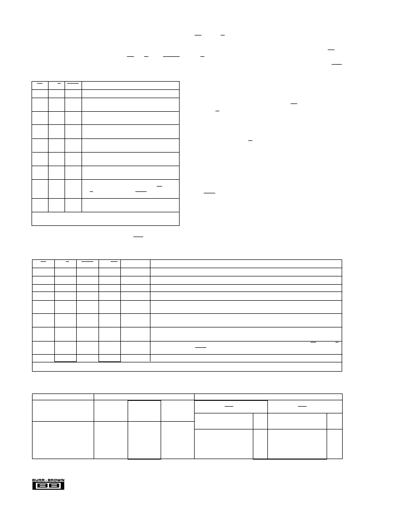
8
ADS7806
CS
R/C
BUSY
OPERATION
1
X
X
None. Databus is in Hi-Z state.
↓
0
1
Initiates conversion “n”. Databus remains
in Hi-Z state.
0
↓
1
Initiates conversion “n”. Databus enters Hi-Z
state.
0
1
↑
Conversion “n” completed. Valid data from
conversion “n” on the databus.
↓
1
1
Enables databus with valid data from
conversion “n”.
↓
1
0
Enables databus with valid data from
conversion “n-1”
(1)
. Conversion n in progress.
0
↑
0
Enables databus with valid data from
conversion “n-1”
(1)
. Conversion “n” in progress.
0
0
↑
New conversion initiated without acquisition
of a new signal. Data will be invalid. CS and/or
R/C must be HIGH when BUSY goes HIGH.
X
X
0
New convert commands ignored. Conversion
“n” in progress.
NOTE: (1) See Figures 2 and 3 for constraints on data valid from
conversion “n-1”.
The ADS7806 will begin tracking the input signal at the end
of the conversion. Allowing 25
μ
s between convert com-
mands assures accurate acquisition of a new signal. Refer to
Tables III and IV for a summary of CS, R/C, and BUSY
states and Figures 2 through 6 for timing diagrams.
CS and R/C are internally OR’d and level triggered. There
is not a requirement which input goes LOW first when
initiating a conversion. If, however, it is critical that CS or
R/C initiates conversion ‘n’, be sure the less critical input is
LOW at least 10ns prior to the initiating input. If EXT/INT
(pin 8) is LOW when initiating conversion ‘n’, serial data
from conversion ‘n-1’ will be output on SDATA (pin 19)
following the start of conversion ‘n’. See
Internal Data
Clock
in the
Reading Data
section.
To reduce the number of control pins, CS can be tied LOW
using R/C to control the read and convert modes. This will
have no effect when using the internal data clock in the serial
output mode. However, the parallel output and the serial
output (only when using an external data clock) will be
affected whenever R/C goes HIGH. Refer to the
Reading
Data
section.
READING DATA
The ADS7806 outputs serial or parallel data in Straight
Binary or Binary Two’s Complement data output format. If
SB/BTC (pin 7) is HIGH, the output will be in SB format,
and if LOW, the output will be in BTC format. Refer to
Table V for ideal output codes.
The parallel output can be read without affecting the internal
output registers; however, reading the data through the serial
Table III. Control Functions When Using Parallel Output
(DATACLK tied LOW, EXT/INT tied HIGH).
CS
R/C
BUSY
EXT/INT
DATACLK
OPERATION
↓
0
1
0
Output
Initiates conversion “n”. Valid data from conversion “n-1” clocked out on SDATA.
0
↓
1
0
Output
Initiates conversion “n”. Valid data from conversion “n-1” clocked out on SDATA.
↓
0
1
1
Input
Initiates conversion “n”. Internal clock still runs conversion process.
0
↓
1
1
Input
Initiates conversion “n”. Internal clock still runs conversion process.
↓
1
1
1
Input
Conversion “n” completed. Valid data from conversion “n” clocked out on SDATA synchronized
to external data clock.
↓
1
0
1
Input
Valid data from conversion “n-1” output on SDATA synchronized to external data clock.
Conversion “n” in progress.
0
↑
0
1
Input
Valid data from conversion “n-1” output on SDATA synchronized to external data clock.
Conversion “n” in progress.
0
0
↑
X
X
New conversion initiated without acquisition of a new signal. Data will be invalid. CS and/or R/C
must be HIGH when BUSY goes HIGH.
X
X
0
X
X
New convert commands ignored. Conversion “n” in progress.
NOTE: (1) See Figures 4, 5, and 6 for constraints on data valid from conversion “n-1”.
Table IV. Control Functions When Using Serial Output.
HEX
HEX
BINARY CODE
CODE
BINARY CODE
CODE
+Full Scale (FS – 1LSB)
9.99512V
4.99878V
3.999024V
0111 1111 1111 1111
7FF
1111 1111 1111 1111
FFF
Midscale
0V
2.5V
2V
0000 0000 0000 0000
000
1000 0000 0000 0000
800
One LSB Below Midscale
–4.88mV
2.49878V
1.999024V
1111 1111 1111 1111
FFF
0111 1111 1111 1111
7FF
–Full Scale
–10V
0V
0V
1000 0000 0000 0000
800
0000 0000 0000 0000
000
DESCRIPTION
ANALOG INPUT
Full-Scale Range
Least Significant Bit (LSB)
±
10
0V to 5V
1.22mV
0V to 4V
976
μ
V
4.88mV
Table V. Output Codes and Ideal Input Voltages.
BINARY TWO’S COMPLEMENT
(SB/BTC LOW)
STRAIGHT BINARY
(SB/BTC HIGH)
DIGITAL OUTPUT
相關(guān)PDF資料 |
PDF描述 |
|---|---|
| ADS7806UB | Low-Power 12-Bit Sampling CMOS ANALOG-to-DIGITAL CONVERTER |
| ADS7815 | 16-Bit 250kHz Sampling CMOS ANALOG-to-DIGITAL CONVERTER |
| ADS7815U | 16-Bit 250kHz Sampling CMOS ANALOG-to-DIGITAL CONVERTER |
| ADS7817 | 12-Bit Differential Input Micro Power Sampling ANALOG-TO-DIGITAL CONVERTER |
| ADS7817B | 12-Bit Differential Input Micro Power Sampling ANALOG-TO-DIGITAL CONVERTER |
相關(guān)代理商/技術(shù)參數(shù) |
參數(shù)描述 |
|---|---|
| ADS7806U | 制造商:Texas Instruments 功能描述:12BIT ADC LOW POWER SERIAL 7806 |
| ADS7806U/1K | 功能描述:模數(shù)轉(zhuǎn)換器 - ADC Low-Power 12-Bit Sampling CMOS RoHS:否 制造商:Texas Instruments 通道數(shù)量:2 結(jié)構(gòu):Sigma-Delta 轉(zhuǎn)換速率:125 SPs to 8 KSPs 分辨率:24 bit 輸入類型:Differential 信噪比:107 dB 接口類型:SPI 工作電源電壓:1.7 V to 3.6 V, 2.7 V to 5.25 V 最大工作溫度:+ 85 C 安裝風(fēng)格:SMD/SMT 封裝 / 箱體:VQFN-32 |
| ADS7806U/1KE4 | 功能描述:模數(shù)轉(zhuǎn)換器 - ADC Low-Power 12-Bit Sampling CMOS RoHS:否 制造商:Texas Instruments 通道數(shù)量:2 結(jié)構(gòu):Sigma-Delta 轉(zhuǎn)換速率:125 SPs to 8 KSPs 分辨率:24 bit 輸入類型:Differential 信噪比:107 dB 接口類型:SPI 工作電源電壓:1.7 V to 3.6 V, 2.7 V to 5.25 V 最大工作溫度:+ 85 C 安裝風(fēng)格:SMD/SMT 封裝 / 箱體:VQFN-32 |
| ADS7806U/1KG4 | 功能描述:模數(shù)轉(zhuǎn)換器 - ADC Low-Power 12-Bit Sampling CMOS RoHS:否 制造商:Texas Instruments 通道數(shù)量:2 結(jié)構(gòu):Sigma-Delta 轉(zhuǎn)換速率:125 SPs to 8 KSPs 分辨率:24 bit 輸入類型:Differential 信噪比:107 dB 接口類型:SPI 工作電源電壓:1.7 V to 3.6 V, 2.7 V to 5.25 V 最大工作溫度:+ 85 C 安裝風(fēng)格:SMD/SMT 封裝 / 箱體:VQFN-32 |
| ADS7806UB | 功能描述:模數(shù)轉(zhuǎn)換器 - ADC Low-Power 12-Bit Sampling CMOS RoHS:否 制造商:Texas Instruments 通道數(shù)量:2 結(jié)構(gòu):Sigma-Delta 轉(zhuǎn)換速率:125 SPs to 8 KSPs 分辨率:24 bit 輸入類型:Differential 信噪比:107 dB 接口類型:SPI 工作電源電壓:1.7 V to 3.6 V, 2.7 V to 5.25 V 最大工作溫度:+ 85 C 安裝風(fēng)格:SMD/SMT 封裝 / 箱體:VQFN-32 |
發(fā)布緊急采購,3分鐘左右您將得到回復(fù)。