- 您現(xiàn)在的位置:買賣IC網(wǎng) > PDF目錄375264 > ADS7806 CMOS Quad 2-Input NOR Gate 14-SOIC -55 to 125 PDF資料下載
參數(shù)資料
| 型號: | ADS7806 |
| 英文描述: | CMOS Quad 2-Input NOR Gate 14-SOIC -55 to 125 |
| 中文描述: | 低功耗12位采樣CMOS模擬數(shù)字轉(zhuǎn)換器 |
| 文件頁數(shù): | 17/18頁 |
| 文件大?。?/td> | 209K |
| 代理商: | ADS7806 |
17
ADS7806
The resistive front end of the ADS7806 also provides a
guaranteed
±
25V overvoltage protection. In most cases, this
eliminates the need for external over voltage protection
circuitry.
INTERMEDIATE LATCHES
The ADS7806 does have tri-state outputs for the parallel
port, but intermediate latches should be used if the bus will
be active during conversions. If the bus is not active during
conversion, the tri-state outputs can be used to isolate the
A/D from other peripherals on the same bus.
Intermediate latches are beneficial on any monolithic A/D
converter. The ADS7806 has an internal LSB size of 610
μ
V.
Transients from fast switching signals on the parallel port,
even when the A/D is tri-stated, can be coupled through the
substrate to the analog circuitry causing degradation of
converter performance. The effects of this phenomenon will
be more obvious when using the pin-compatible ADS7807
or any of the other 16-bit converters in the ADS Family. This
is due to the smaller internal LSB size of 38
μ
V.
APPLICATIONS INFORMATION
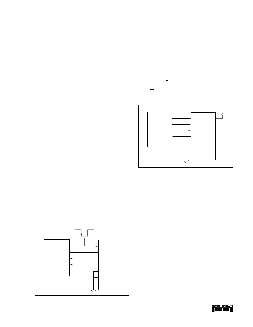
QSPI INTERFACING
Figure 12 shows a simple interface between the ADS7806
and any QSPI equipped microcontroller. This interface as-
sumes that the convert pulse does not originate from the
microcontroller and that the ADS7806 is the only serial
peripheral.
Before enabling the QSPI interface, the microcontroller
must be configured to monitor the slave select line. When a
transition from LOW to HIGH occurs on Slave Select (SS)
from BUSY (indicating the end of the current conversion),
the port can be enabled. If this is not done, the microcontroller
and the and the A/D may be “out-of-sync.”
Figure 13 shows another interface between the ADS7806
and a QSPI equipped microcontroller. The interface allows
the microcontroller to give the convert pulses while also
allowing multiple peripherals to be connected to the serial
bus. This interface and the following discussion assume a
master clock for the QSPI interface of 16.78MHz. Notice
that the serial data input of the microcontroller is tied to the
MSB (D7) of the ADS7806 instead of the serial output
(SDATA). Using D7 instead of the serial port offers tri-state
capability which allows other peripherals to be connected to
the MISO pin. When communication is desired with those
peripherals, PCS0 and PCS1 should be left HIGH; that will
keep D7 tri-stated and prevent a conversion from taking
place.
In this configuration, the QSPI interface is actually set to do
two different serial transfers. The first, an eight bit transfer,
causes PCS0 (R/C) and PCS1 (CS) to go LOW starting a
conversion. The second, a twelve bit transfer, causes only
PCS1 (CS) to go LOW. This is when the valid data will be
transferred.
For both transfers, the DT register (delay after transfer) is
used to cause a 19
μ
s delay. The interface is also set up to
wrap to the beginning of the queue. In this manner, the QSPI
is a state machine which generates the appropriate timing for
the ADS7806. This timing is thus locked to the crystal based
timing of the microcontroller and not interrupt driven. So,
this interface is appropriate for both AC and DC measure-
ments.
For the fastest conversion rate, the baud rate should be set to
two (4.19MHz SCK), DT set to ten, the first serial transfer
set to eight bits, the second set to twelve bits, and DSCK
disabled (in the command control byte). This will allow for
a 23kHz maximum conversion rate. For slower rates, DT
should be increased. Do not slow SCK as this may increase
the chance of affecting the conversion results or accidently
initiating a second conversion during the first eight bit
transfer.
In addition, CPOL and CPHA should be set to zero (SCK
normally LOW and data captured on the rising edge). The
command control byte for the eight bit transfer should be set
to 20H and for the twelve bit transfer to 61H.
FIGURE 13. QSPI Interface to the ADS7806. Processor
Initiates Conversions.
R/C
CS
DATACLK
D7 (MSB)
BYTE
ADS7806
PCS0
PCS1
SCK
MISO
QSPI
CPOL = 0
CPHA = 0
EXT/INT
+5V
FIGURE 12. QSPI Interface to the ADS7806.
R/C
BUSY
SDATA
DATACLK
CS
EXT/INT
BYTE
ADS7806
PCS0/SS
MOSI
SCK
QSPI
CPOL = 0 (Inactive State is LOW)
CPHA = 1 (Data valid on falling edge)
QSPI port is in slave mode.
Convert Pulse
相關(guān)PDF資料 |
PDF描述 |
|---|---|
| ADS7806P | CMOS Quad 2-Input NOR Gate 14-SOIC -55 to 125 |
| ADS7806PB | Low-Power 12-Bit Sampling CMOS ANALOG-to-DIGITAL CONVERTER |
| ADS7806U | Low-Power 12-Bit Sampling CMOS ANALOG-to-DIGITAL CONVERTER |
| ADS7806UB | Low-Power 12-Bit Sampling CMOS ANALOG-to-DIGITAL CONVERTER |
| ADS7815 | 16-Bit 250kHz Sampling CMOS ANALOG-to-DIGITAL CONVERTER |
相關(guān)代理商/技術(shù)參數(shù) |
參數(shù)描述 |
|---|---|
| ADS7806P | 功能描述:模數(shù)轉(zhuǎn)換器 - ADC Low-Power 12-Bit Sampling CMOS RoHS:否 制造商:Texas Instruments 通道數(shù)量:2 結(jié)構(gòu):Sigma-Delta 轉(zhuǎn)換速率:125 SPs to 8 KSPs 分辨率:24 bit 輸入類型:Differential 信噪比:107 dB 接口類型:SPI 工作電源電壓:1.7 V to 3.6 V, 2.7 V to 5.25 V 最大工作溫度:+ 85 C 安裝風(fēng)格:SMD/SMT 封裝 / 箱體:VQFN-32 |
| ADS7806P | 制造商:BURR-BROWN 功能描述:12BIT ADC SAMPLING 7806 DIP28 |
| ADS7806PB | 功能描述:模數(shù)轉(zhuǎn)換器 - ADC Low-Power 12-Bit Sampling CMOS RoHS:否 制造商:Texas Instruments 通道數(shù)量:2 結(jié)構(gòu):Sigma-Delta 轉(zhuǎn)換速率:125 SPs to 8 KSPs 分辨率:24 bit 輸入類型:Differential 信噪比:107 dB 接口類型:SPI 工作電源電壓:1.7 V to 3.6 V, 2.7 V to 5.25 V 最大工作溫度:+ 85 C 安裝風(fēng)格:SMD/SMT 封裝 / 箱體:VQFN-32 |
| ADS7806PBG4 | 功能描述:模數(shù)轉(zhuǎn)換器 - ADC Low-Power 12-Bit Sampling CMOS RoHS:否 制造商:Texas Instruments 通道數(shù)量:2 結(jié)構(gòu):Sigma-Delta 轉(zhuǎn)換速率:125 SPs to 8 KSPs 分辨率:24 bit 輸入類型:Differential 信噪比:107 dB 接口類型:SPI 工作電源電壓:1.7 V to 3.6 V, 2.7 V to 5.25 V 最大工作溫度:+ 85 C 安裝風(fēng)格:SMD/SMT 封裝 / 箱體:VQFN-32 |
| ADS7806PG4 | 功能描述:模數(shù)轉(zhuǎn)換器 - ADC Low-Power 12-Bit Sampling CMOS RoHS:否 制造商:Texas Instruments 通道數(shù)量:2 結(jié)構(gòu):Sigma-Delta 轉(zhuǎn)換速率:125 SPs to 8 KSPs 分辨率:24 bit 輸入類型:Differential 信噪比:107 dB 接口類型:SPI 工作電源電壓:1.7 V to 3.6 V, 2.7 V to 5.25 V 最大工作溫度:+ 85 C 安裝風(fēng)格:SMD/SMT 封裝 / 箱體:VQFN-32 |
發(fā)布緊急采購,3分鐘左右您將得到回復(fù)。