- 您現(xiàn)在的位置:買賣IC網 > PDF目錄374023 > ADP3801 (Analog Devices, Inc.) High Frequency Switch Mode Dual Li-Ion Battery Chargers(高頻開關模式雙鋰離子充電器) PDF資料下載
參數(shù)資料
| 型號: | ADP3801 |
| 廠商: | Analog Devices, Inc. |
| 元件分類: | 基準電壓源/電流源 |
| 英文描述: | High Frequency Switch Mode Dual Li-Ion Battery Chargers(高頻開關模式雙鋰離子充電器) |
| 中文描述: | 高頻開關雙鋰離子電池充電器(高頻開關模式雙鋰離子充電器) |
| 文件頁數(shù): | 14/20頁 |
| 文件大?。?/td> | 278K |
| 代理商: | ADP3801 |
ADP3801/ADP3802
–14–
REV. 0
Gate Drive
The ADP3801 and ADP3802 are designed to directly drive the
gate of a PFET with no additional circuitry as shown on the
circuit diagram. The DRV pin pulls the gate up to within
250 mV of VCC, which is more than enough to ensure that the
transistor turns off. To turn the PFET on, the DRV pin pulls
down to a clamped voltage that is at most 7V below VCC. Check
the specified PFET’s maximum Gate-Source rating to see if this
voltage does not exceed its breakdown. The Si4463 is rated at
V
GSMAX
= 12 V, which is well above the maximum gate drive for
the ADP3801/ADP3802.
Schottky Rectifier Selection and Thermal Design
The Schottky diode’s peak current and average power dissipa-
tion must not exceed the diode ratings. The most stressful con-
dition for the output diode is under short circuit (V
O
= 0 V),
where the diode duty cycle D
D
is at least 95%. Under this con-
dition, the diode must safely handle I
PK
at close to 100% duty
cycle.
The diode power dissipation (P
D
) is calculated by multiplying
the forward voltage drop (V
F
) times the Schottky diode duty
cycle multiplied by the short circuit current. The worst-case
forward voltage drop of MBRD835 diode is 0.41 V at I
PK
=
4.5 A, thus:
P
D
=
I
PK
×
D
D
×
V
F
= 4.5
×
0.95
×
0.41 = 1.8
W
From the diode’s worst-case dissipation, the maximum junction
temperature T
JMAX
of the diode can be calculated:
T
J
MAX
=
T
A
+
R
θ
J
A
×
P
D
= 25 + (40)
×
1.8 = 97
°
C
R
θ
J
A
is the junction to ambient thermal impedance of the diode.
The calculated T
JMAX
should be below the maximum allowed
junction temperature of the diode with adequate margin. T
JMAX
of the MBRD835 is 125
°
C, which is met with adequate margin.
Input Capacitor Selection
In continuous mode, the source current of the PMOS is a square
wave of duty cycle V
OUT
/V
IN
. To prevent large voltage tran-
sients, a low ESR input capacitor sized for the maximum rms
current must be used. The maximum rms capacitor current is
given by:
I
I
V
V
V
(
V
RMS
OUT
IN
OUT
IN
OUT
≈
×
)
This formula has a maximum at
V
IN
= 2
V
OUT
, where
I
RMS
=
I
OUT
/2 = 2.0 A.
This simple worst case condition is commonly used for design
because even significant deviations do not offer much relief.
Note that capacitor manufacturers’ ripple current ratings are
often based on only 2000 hours of life. This makes it advisable
to further derate the capacitor, or to choose a capacitor rated at
a higher temperature than required. Several capacitors may also
be paralleled to meet size or height requirements in the design.
As a first choice, three 68
μ
F/20 V Sprague type 593D tantalum
capacitors are used in parallel. Each is specified as follows:
ESR = 0.2
, maximum ripple current of 0.91A
RMS
. In addition
to C
IN
, a 0.1
μ
F decoupling capacitor is required as close as
possible to the VCC pin.
Once the capacitor is chosen, the input ripple voltage should be
checked:
This is low enough for most applications. For cost reduction,
one of the 68
μ
F capacitors could be removed, or a cheaper
electrolytic could be used instead.
V
I
ESR
D
f
C
A
kHz
F
mV
INRIPPLE
O
ON
OSC
IN
PP
=
×
+
×
=
×
+
×
=
/
.
.
/
100
4 0
0 07
84 100
200
210
360
μ
Output Capacitor Selection
As a first choice, we’ll use two of the same type of 68
μ
F
Sprague capacitors for the output. The inductor rms ripple current
was calculated as 0.3 A, which is far below the specification for
these capacitors. The other consideration is the allowable output
ripple voltage. Assuming high battery internal resistance, all of
the worst case inductor ripple current may flow through the
output capacitor. This results in a ripple voltage of:
This ripple is low enough for most applications. Again, one of
the capacitors could be removed or lower cost electrolytic ca-
pacitors could be used to reduce cost.
V
I
ESR
D
f
C
A
kHz
F
mV
OUTRIPPLE
LPP
ON
OSC
OUT
PP
=
×
+
×
=
×
+
×
=
/
.
.
/
100
1 0
0 1
84 100
200
140
130
μ
Charger Performance Summary
The circuit properly executes the charging algorithm, exhibiting
stable operation regardless of battery conditions, including an
open circuit load in which the battery is removed.
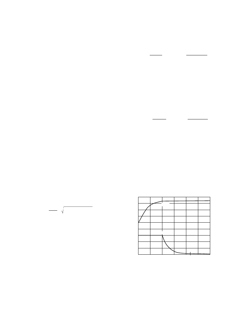
Li-Ion charging characteristics are given in Figure 25. The
charge current is maintained at its programmed level until the
battery reaches its final voltage. Then the current begins to
decrease. The shape of the current decrease is dependent on the
internal impedance of the battery. When the current drops below
240 mA, the
EOC
comparator signals the end-of-charge of the
battery.
TIME – Hours
I
C
0
0.5
1.0
1.5
2.0
3.0
3.0
3.5
4.0
2.5
V
B
0
1.3
2.7
4.0
2.5
4.5
V
BAT
I
CHARGE
EOC
Figure 25. Li-Ion Charging Characteristic
相關PDF資料 |
PDF描述 |
|---|---|
| ADP3802 | High Frequency Switch Mode Dual Li-Ion Battery Chargers(高頻開關模式雙鋰離子充電器) |
| ADP3804JRU-125 | Aluminum Electrolytic Radial Leaded Bi-Polar Capacitor; Capacitance: 220uF; Voltage: 35V; Case Size: 12.5x20 mm; Packaging: Bulk |
| ADP3804JRU-126 | Aluminum Electrolytic Radial Leaded Bi-Polar Capacitor; Capacitance: 330uF; Voltage: 35V; Case Size: 12.5x20 mm; Packaging: Bulk |
| ADP3804 | Secondary Over-Voltage Protection for 2-4 cell in series Li-Ion/Poly (4.50V) 8-TSSOP -40 to 110 |
| ADP3804JRU | Secondary Over-Voltage Protection for 2-4 cell in series Li-Ion/Poly (4.50V) 8-TSSOP -40 to 110 |
相關代理商/技術參數(shù) |
參數(shù)描述 |
|---|---|
| ADP38010001RR | 制造商:Rochester Electronics LLC 功能描述:- Bulk |
| ADP3801AR | 制造商:Analog Devices 功能描述: |
| ADP3801AR-REEL | 制造商:Rochester Electronics LLC 功能描述:SWITCH MODE DUAL CHARGER/LDO REGULATOR - Tape and Reel |
| ADP3802 | 制造商:AD 制造商全稱:Analog Devices 功能描述:High Frequency Switch Mode Dual Li-Ion Battery Chargers |
| ADP3802AR | 制造商:AD 制造商全稱:Analog Devices 功能描述:High Frequency Switch Mode Dual Li-Ion Battery Chargers |
發(fā)布緊急采購,3分鐘左右您將得到回復。