- 您現(xiàn)在的位置:買賣IC網(wǎng) > PDF目錄373993 > ADL5372 (Analog Devices, Inc.) 300 MHz to 1000 MHz Quadrature Modulator PDF資料下載
參數(shù)資料
| 型號: | ADL5372 |
| 廠商: | Analog Devices, Inc. |
| 英文描述: | 300 MHz to 1000 MHz Quadrature Modulator |
| 中文描述: | 300 MHz到1000 MHz的正交調(diào)制器 |
| 文件頁數(shù): | 11/20頁 |
| 文件大小: | 904K |
| 代理商: | ADL5372 |
ADL5370
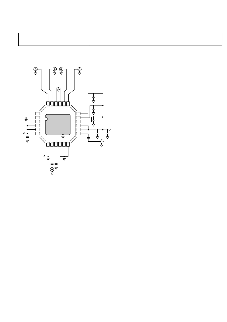
BASIC CONNECTIONS
Figure 25 shows the basic connections for the ADL5370.
Rev. 0 | Page 11 of 20
VPS5
VPS3
VPS4
VPS2
VPS2
VOUT
C
L
L
C
C
C
Q
C
Q
C
I
I
0
COM1
VPS1
COM1
VPS1
VPS1
VPS1
1
2
3
4
5
6
18
17
16
15
14
13
VOUT
C13
0.1μF
C11
OPEN
C12
0.1μF
CLON
100pF
C14
0.1μF
C15
0.1μF
C16
0.1μF
2
2
2
2
2
1
7
8
9
1
1
1
COUT
100pF
VPOS
V
QBBP
QBBN
IBBN
IBBP
EXPOSED PADDLE
CLOP
100pF
LO
GND
Z1
ADL5370
Figure 25. Basic Connections for the ADL5370
Power Supply and Grounding
All the VPS pins must be connected to the same 5 V source.
Adjacent pins of the same name can be tied together and decoupled
with a 0.1 μF capacitor. These capacitors should be located as
close as possible to the device. The power supply can range
between 4.75 V and 5.25 V.
The COM1 pin, COM2 pin, COM3 pin, and COM4 pin should
be tied to the same ground plane through low impedance paths.
The exposed paddle on the underside of the package should also
be soldered to a low thermal and electrical impedance ground
plane. If the ground plane spans multiple layers on the circuit
board, they should be stitched together with nine vias under the
exposed paddle. The Analog Devices
AN-772
application note
discusses the thermal and electrical grounding of the
LFCSP_VQ in greater detail.
Baseband Inputs
The baseband inputs QBBP, QBBN, IBBP, and IBBN must be
driven from a differential source. The nominal drive level of
1.4 V p-p differential (700 mV p-p on each pin) should be
biased to a common-mode level of 500 mV dc.
The dc common-mode bias level for the baseband inputs may
range from 400 mV to 600 mV. This results in a reduction in
the usable input ac swing range. The nominal dc bias of 500 mV
allows for the largest ac swing, limited on the bottom end by the
ADL5370 input range and on the top end by the output compliance
range on most digital-to-analog converters (DAC) from Analog
Devices.
LO Input
A single-ended LO signal should be applied to the LOIP pin
through an ac-coupling capacitor. The recommended LO drive
power is 0 dBm. The LO return pin, LOIN, should be ac-coupled
to ground through a low impedance path.
The nominal LO drive of 0 dBm can be increased to up to 7 dBm
to realize an improvement in the noise performance of the
modulator. This improvement is tempered by degradation in
the sideband suppression performance (see Figure 20) and,
therefore, should be used judiciously. If the LO source cannot
provide the 0 dBm level, then operation at a reduced power
below 0 dBm is acceptable. Reduced LO drive results in slightly
increased modulator noise. The effect of LO power on sideband
suppression and carrier feedthrough is shown in Figure 20. The
effect of LO power on GSM noise is shown in Figure 35.
RF Output
The RF output is available at the VOUT pin (Pin 13). This pin
must also be ac-coupled. The VOUT pin has a nominal
broadband impedance of 50 Ω and does not need further
external matching.
相關PDF資料 |
PDF描述 |
|---|---|
| ADL5373 | 300 MHz to 1000 MHz Quadrature Modulator |
| ADL5374 | 300 MHz to 1000 MHz Quadrature Modulator |
| ADL5385 | 300 MHz to 1000 MHz Quadrature Modulator |
| ADL5370 | 300 MHz to 1000 MHz Quadrature Modulator |
| ADL5370ACPZ-R2 | 300 MHz to 1000 MHz Quadrature Modulator |
相關代理商/技術參數(shù) |
參數(shù)描述 |
|---|---|
| ADL5372ACPZ-R2 | 制造商:Analog Devices 功能描述:1500 MHZ TO 2500 MHZ QUADRATURE MODULATOR - Tape and Reel |
| ADL5372ACPZ-R21 | 制造商:AD 制造商全稱:Analog Devices 功能描述:1500 MHz to 2500 MHz Quadrature Modulator |
| ADL5372ACPZ-R7 | 功能描述:IC QUADRA MOD 1.5/2.5GHZ 24LFCSP RoHS:是 類別:RF/IF 和 RFID >> RF 調(diào)制器 系列:- 產(chǎn)品培訓模塊:Lead (SnPb) Finish for COTS Obsolescence Mitigation Program 標準包裝:2,500 系列:- 功能:調(diào)制器 LO 頻率:700MHz ~ 2.3GHz RF 頻率:700MHz ~ 2.3GHz P1dB:1dBm 底噪:-148dBm/Hz 輸出功率:-1dBm 電流 - 電源:46mA 電源電壓:2.7 V ~ 3.6 V 測試頻率:1.75GHz 封裝/外殼:28-WFQFN 裸露焊盤 包裝:帶卷 (TR) |
| ADL5372ACPZ-R71 | 制造商:AD 制造商全稱:Analog Devices 功能描述:1500 MHz to 2500 MHz Quadrature Modulator |
| ADL5372ACPZ-WP | 制造商:Analog Devices 功能描述:QUADRATURE MOD 700MHZ 24LFCSP EP - Waffle Pack |
發(fā)布緊急采購,3分鐘左右您將得到回復。