- 您現(xiàn)在的位置:買賣IC網(wǎng) > PDF目錄373979 > ADE7169ACPZF16 (ANALOG DEVICES INC) Single-Phase Energy Measurement IC with 8052 MCU, RTC and LCD driver PDF資料下載
參數(shù)資料
| 型號: | ADE7169ACPZF16 |
| 廠商: | ANALOG DEVICES INC |
| 元件分類: | 模擬信號調(diào)理 |
| 英文描述: | Single-Phase Energy Measurement IC with 8052 MCU, RTC and LCD driver |
| 中文描述: | SPECIALTY ANALOG CIRCUIT, QCC64 |
| 封裝: | 9 X 9 MM, ROHS COMPLIANT, MO-22-VMMD-4, LFCSP-64 |
| 文件頁數(shù): | 64/140頁 |
| 文件大小: | 1359K |
| 代理商: | ADE7169ACPZF16 |
第1頁第2頁第3頁第4頁第5頁第6頁第7頁第8頁第9頁第10頁第11頁第12頁第13頁第14頁第15頁第16頁第17頁第18頁第19頁第20頁第21頁第22頁第23頁第24頁第25頁第26頁第27頁第28頁第29頁第30頁第31頁第32頁第33頁第34頁第35頁第36頁第37頁第38頁第39頁第40頁第41頁第42頁第43頁第44頁第45頁第46頁第47頁第48頁第49頁第50頁第51頁第52頁第53頁第54頁第55頁第56頁第57頁第58頁第59頁第60頁第61頁第62頁第63頁當(dāng)前第64頁第65頁第66頁第67頁第68頁第69頁第70頁第71頁第72頁第73頁第74頁第75頁第76頁第77頁第78頁第79頁第80頁第81頁第82頁第83頁第84頁第85頁第86頁第87頁第88頁第89頁第90頁第91頁第92頁第93頁第94頁第95頁第96頁第97頁第98頁第99頁第100頁第101頁第102頁第103頁第104頁第105頁第106頁第107頁第108頁第109頁第110頁第111頁第112頁第113頁第114頁第115頁第116頁第117頁第118頁第119頁第120頁第121頁第122頁第123頁第124頁第125頁第126頁第127頁第128頁第129頁第130頁第131頁第132頁第133頁第134頁第135頁第136頁第137頁第138頁第139頁第140頁
ADE7169F16
Preliminary Technical Data
proportional to Active power, reactive power, or Apparent/Irms
respectively.
Rev. PrD | Page 64 of 140
The selection between Irms and Apparent power is done by the
VARMSCFCON bit in the MODE2 register (0x0C). With this
selection, CF2 cannot be proportional to apparent power if CF1
is proportional to Irms and vice-versa.
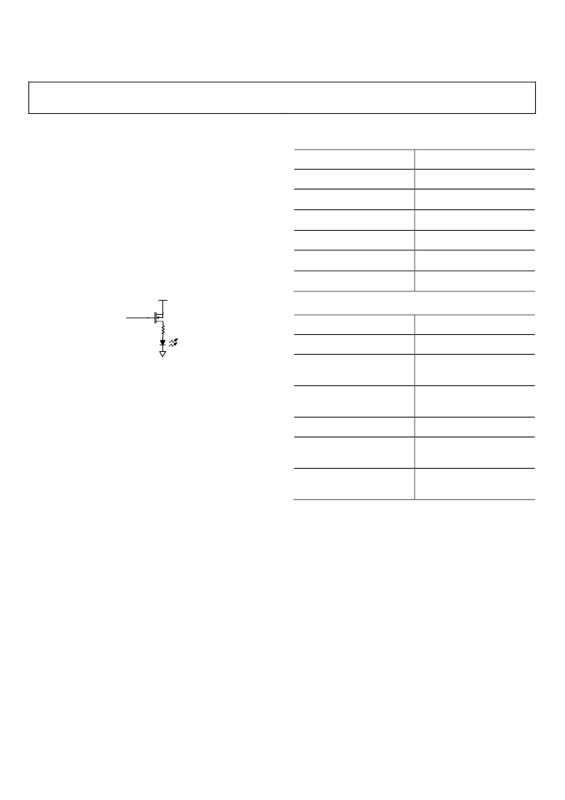
Pulse output characteristic
The pulse output for both DFC stays low for 90ms if the pulse
period is larger than 180ms (5.56Hz). If the pulse period is
smaller than 180ms, the duty cycle of the pulse output is 50%.
The pulse output is active low and should be preferably
connected to an LED as shown on
Figure 53
.
CF
VDD
Figure 53. CF Pulse output
The maximum output frequency, with ac input signals at full
scale and CFxNUM = 0x00 and CFxDEN = 0x00, is
approximately 21.1 kHz.
The ADE7169F16 incorporates two registers, CFxNUM[15:0]
and CFxDEN[15:0] per DFC, to set the CFx frequency. These
are unsigned 16-bit registers, which can be used to adjust the
CFx frequency to a wide range of values. These frequency-
scaling registers are 16-bit registers, which can scale the output
frequency by 1/2
16
to 1 with a step of 1/2
16
.
If the value 0 is written to any of these registers, the value 1
would be applied to the register. The ratio CFxNUM / CFxDEN
should be smaller than 1 to ensure proper operation. If the ratio
of the registers CFxNUM / CFxDEN is greater than 1, the register
values would be adjusted to a ratio of 1. For example, if the
output frequency is 1.562 kHz while the contents of CFxDEN
are 0 (0x000), then the output frequency can be set to 6.1 Hz by
writing 0xFF to the CFxDEN register.
ENERGY REGISTER SCALING
The ADE7169F16 provides measurements of active, reactive,
and apparent energies that use separate paths and filtering for
calculation. The difference in data paths can result in small
differences in LSB weight between active, reactive and apparent
energy registers. These measurements are internally
compensated so the scaling is nearly one to one. The
relationship between the registers is show in Table 42. In Table
43, the relationship between WATTGAIN, VARGAIN and
VAGAIN is given. These relationships can be used for
calibration and simplify the adjustment of VAR and VA gains.
As VAR and VA gains can be deducted from WGAIN, there is
no need to do reactive or apparent gai adjustment.
Table 42. Energy Registers scaling
Line Frequency = 50Hz
Line Frequency = 60Hz
Integrator OFF
VAR = 0.9952
×
WATT
VAR = 0.9949
×
WATT
VA = 0.9978
×
WATT
VA = 1.0015
×
WATT
Integrator ON
VAR = 0.9997
×
WATT
VAR = 0.9999
×
WATT
VA = 0.9977
×
WATT
Table 43. Gain compensation adjustments
Line Frequency = 50Hz
VA = 1.0015
×
WATT
Line Frequency = 60Hz
Integrator OFF
VARGAIN = 19.76 +
WGAIN/0.9952
VARGAIN = 21 +
WGAIN/0.9949
VAGAIN = 9.03 +
WGAIN/0.9978
VAGAIN = -60.53 +
WGAIN/1.0015
Integrator ON
VARGAIN = 1.23 +
WGAIN/0.9997
VARGAIN = 0.41 +
WGAIN/0.9999
VAGAIN = 9.44 +
WGAIN/0.9977
VAGAIN = -60.53 +
WGAIN/1.0015
ENERGY MEASUREMENT INTERRUPTS
The Energy Measurement part of the ADE7169F16 has its own
interrupt vector for the 8052 core – Vector address 0x004B – see
Interrupt Vectors section. The bits set in the Interrupt Enable
Register 1 SFR (MIRQENL, 0xD9), Interrupt Enable Register 2
SFR (MIRQENM, 0xDA), and Interrupt Enable Register 3 SFR
(MIRQENH, 0xDB) enables the energy measurement interrupts
that are allowed to interrupt the 8052 core. If an event is not
enabled, it cannot create a system interrupt.
The ADE interrupt stays active until the status bit that has
created the interrupt is cleared. Two methods can be used to
clear the ADE interrupt:
- When bit 6 (ADEIAUTCLR) of the Power Management
Interrupt Enable SFR (IPSME, 0xEC) is set, all the status bits of
the ADE irq status register (1, 2 or 3) are cleared when the
register is read.
- When bit 6 (ADEIAUTCLR) of the Power Management
相關(guān)PDF資料 |
PDF描述 |
|---|---|
| ADE7169ACPZF16-RL | Single-Phase Energy Measurement IC with 8052 MCU, RTC and LCD driver |
| ADE7169ASTF16 | Single-Phase Energy Measurement IC with 8052 MCU, RTC and LCD driver |
| ADE7169ASTF16-RL | Single-Phase Energy Measurement IC with 8052 MCU, RTC and LCD driver |
| ADE7169ASTZF16 | Single-Phase Energy Measurement IC with 8052 MCU, RTC and LCD driver |
| ADE7169ASTZF16-RL | Single-Phase Energy Measurement IC with 8052 MCU, RTC and LCD driver |
相關(guān)代理商/技術(shù)參數(shù) |
參數(shù)描述 |
|---|---|
| ADE7169ACPZF161 | 制造商:AD 制造商全稱:Analog Devices 功能描述:Single-Phase Energy Measurement IC with 8052 MCU, RTC and LCD driver |
| ADE7169ACPZF16-RL | 制造商:AD 制造商全稱:Analog Devices 功能描述:Single-Phase Energy Measurement IC with 8052 MCU, RTC, and LCD Driver |
| ADE7169ACPZF16-RL1 | 制造商:AD 制造商全稱:Analog Devices 功能描述:Single-Phase Energy Measurement IC with 8052 MCU, RTC and LCD driver |
| ADE7169ASTF16 | 制造商:AD 制造商全稱:Analog Devices 功能描述:Single-Phase Energy Measurement IC with 8052 MCU, RTC and LCD driver |
| ADE7169ASTF16-RL | 制造商:AD 制造商全稱:Analog Devices 功能描述:Single-Phase Energy Measurement IC with 8052 MCU, RTC and LCD driver |
發(fā)布緊急采購,3分鐘左右您將得到回復(fù)。