- 您現(xiàn)在的位置:買賣IC網(wǎng) > PDF目錄373979 > ADE7169ACPZF16 (ANALOG DEVICES INC) Single-Phase Energy Measurement IC with 8052 MCU, RTC and LCD driver PDF資料下載
參數(shù)資料
| 型號(hào): | ADE7169ACPZF16 |
| 廠商: | ANALOG DEVICES INC |
| 元件分類: | 模擬信號(hào)調(diào)理 |
| 英文描述: | Single-Phase Energy Measurement IC with 8052 MCU, RTC and LCD driver |
| 中文描述: | SPECIALTY ANALOG CIRCUIT, QCC64 |
| 封裝: | 9 X 9 MM, ROHS COMPLIANT, MO-22-VMMD-4, LFCSP-64 |
| 文件頁(yè)數(shù): | 136/140頁(yè) |
| 文件大小: | 1359K |
| 代理商: | ADE7169ACPZF16 |
第1頁(yè)第2頁(yè)第3頁(yè)第4頁(yè)第5頁(yè)第6頁(yè)第7頁(yè)第8頁(yè)第9頁(yè)第10頁(yè)第11頁(yè)第12頁(yè)第13頁(yè)第14頁(yè)第15頁(yè)第16頁(yè)第17頁(yè)第18頁(yè)第19頁(yè)第20頁(yè)第21頁(yè)第22頁(yè)第23頁(yè)第24頁(yè)第25頁(yè)第26頁(yè)第27頁(yè)第28頁(yè)第29頁(yè)第30頁(yè)第31頁(yè)第32頁(yè)第33頁(yè)第34頁(yè)第35頁(yè)第36頁(yè)第37頁(yè)第38頁(yè)第39頁(yè)第40頁(yè)第41頁(yè)第42頁(yè)第43頁(yè)第44頁(yè)第45頁(yè)第46頁(yè)第47頁(yè)第48頁(yè)第49頁(yè)第50頁(yè)第51頁(yè)第52頁(yè)第53頁(yè)第54頁(yè)第55頁(yè)第56頁(yè)第57頁(yè)第58頁(yè)第59頁(yè)第60頁(yè)第61頁(yè)第62頁(yè)第63頁(yè)第64頁(yè)第65頁(yè)第66頁(yè)第67頁(yè)第68頁(yè)第69頁(yè)第70頁(yè)第71頁(yè)第72頁(yè)第73頁(yè)第74頁(yè)第75頁(yè)第76頁(yè)第77頁(yè)第78頁(yè)第79頁(yè)第80頁(yè)第81頁(yè)第82頁(yè)第83頁(yè)第84頁(yè)第85頁(yè)第86頁(yè)第87頁(yè)第88頁(yè)第89頁(yè)第90頁(yè)第91頁(yè)第92頁(yè)第93頁(yè)第94頁(yè)第95頁(yè)第96頁(yè)第97頁(yè)第98頁(yè)第99頁(yè)第100頁(yè)第101頁(yè)第102頁(yè)第103頁(yè)第104頁(yè)第105頁(yè)第106頁(yè)第107頁(yè)第108頁(yè)第109頁(yè)第110頁(yè)第111頁(yè)第112頁(yè)第113頁(yè)第114頁(yè)第115頁(yè)第116頁(yè)第117頁(yè)第118頁(yè)第119頁(yè)第120頁(yè)第121頁(yè)第122頁(yè)第123頁(yè)第124頁(yè)第125頁(yè)第126頁(yè)第127頁(yè)第128頁(yè)第129頁(yè)第130頁(yè)第131頁(yè)第132頁(yè)第133頁(yè)第134頁(yè)第135頁(yè)當(dāng)前第136頁(yè)第137頁(yè)第138頁(yè)第139頁(yè)第140頁(yè)
ADE7169F16
Preliminary Technical Data
Bit Location
Rev. PrD | Page 136 of 140
Bit
Addr.
0x87
0x86
0x85
0x84
0x83
0x82
0x81
0x80
Bit
Name
T1
T0
CF2
CF1
INT1
Default
Value
1
1
1
1
1
1
1
1
Description
7
6
5
4
3
2
1
0
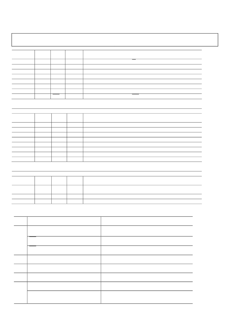
Table 139. Port 1 SFR (P1, 0x90)
Note: When an alternate function is chosen for a pin of this port, the bit controlling this pin should always be set
Bit Location
Bit
Addr.
Name
value
7
0x97
1
This bit reflects the state of P1.7 pin. It can be written or read.
6
0x96
1
This bit reflects the state of P1.6 pin. It can be written or read.
5
0x95
1
This bit reflects the state of P1.5 pin. It can be written or read.
4
0x94
T2
1
This bit reflects the state of P1.4/T2 pin. It can be written or read.
3
0x93
T2EX
1
This bit reflects the state of P1.3/T2EX pin. It can be written or read.
2
0x92
1
This bit reflects the state of P1.2 pin. It can be written or read.
1
0x91
TxD
1
This bit reflects the state of P1.1/TxD pin. It can be written or read.
0
0x90
RxD
1
This bit reflects the state of P1.0/RxD pin. It can be written or read.
Table 140. Port 2 SFR (P2, 0xA0)
Note: When an alternate function is chosen for a pin of this port, the bit controlling this pin should always be set
Bit Location
Bit
Addr.
Name
Value
7 - 2
0x97 –
0x92
1
0x91
P2.1
1
This bit reflects the state of P2.1 pin. It can be written or read.
0
0x90
P2.0
1
This bit reflects the state of P2.0 pin. It can be written or read.
This bit reflects the state of P0.7/SS/T1 pin. It can be written or read.
This bit reflects the state of P0.6/SCLK/T0 pin. It can be written or read.
This bit reflects the state of P0.5/MISO pin. It can be written or read.
This bit reflects the state of P0.4/MOSI/SDATA pin. It can be written or read.
This bit reflects the state of P0.3/CF2 pin. It can be written or read.
This bit reflects the state of P0.2/CF1 pin. It can be written or read.
This bit reflects the state of P0.1 pin. It can be written or read.
This bit reflects the state of P0.0/INT1/BCTRL pin. It can be written or read.
Bit
Default
Description
Bit
Default
Description
0x3F
These bits are unused and should be left set
Table 141. Port 0 Alternate Functions
Pin
No.
BCTRL external battery control input
P0.0
Alternate Function
Alternate Function Enable
Set INT1PROG[2:0]=X01 in the Interrupt pins configuration
SFR (INTPR, 0xFF)
INT1 external interrupt
Set EX1 in the Interrupt Enable SFR (IE, 0xA8).
INT1 wakeup from PSM2 operating mode
Set INT1PROG[2:0]=11X in the Interrupt pins configuration
SFR (INTPR, 0xFF)
Set FP19EN in the LCD Segment Enable 2 SFR (LCDSEGE2,
0xED)
Clear the DISCF1 bit in the ADE energy measurement
internal MODE1 register (0x0B)
Clear the DISCF2 bit in the ADE energy measurement
internal MODE1 register (0x0B)
Set the SCPS bit in the CFG SFR and set the SPIEN bit in the
SPI Configuration Register SFR (SPIMOD1, 0xE8).
Clear the SCPS bit in the Configuration SFR (CFG, 0xAF) and
set the I2CEN bit in the I2C Mode Register SFR (I2CMOD,
0xE8).
P0.1
FP19 LCD Segment Pin
P0.2
CF1 ADE Calibration Frequency output
P0.3
CF2 ADE Calibration Frequency output
MOSI SPI Data line
P0.4
SDATA I
2
C Data line
相關(guān)PDF資料 |
PDF描述 |
|---|---|
| ADE7169ACPZF16-RL | Single-Phase Energy Measurement IC with 8052 MCU, RTC and LCD driver |
| ADE7169ASTF16 | Single-Phase Energy Measurement IC with 8052 MCU, RTC and LCD driver |
| ADE7169ASTF16-RL | Single-Phase Energy Measurement IC with 8052 MCU, RTC and LCD driver |
| ADE7169ASTZF16 | Single-Phase Energy Measurement IC with 8052 MCU, RTC and LCD driver |
| ADE7169ASTZF16-RL | Single-Phase Energy Measurement IC with 8052 MCU, RTC and LCD driver |
相關(guān)代理商/技術(shù)參數(shù) |
參數(shù)描述 |
|---|---|
| ADE7169ACPZF161 | 制造商:AD 制造商全稱:Analog Devices 功能描述:Single-Phase Energy Measurement IC with 8052 MCU, RTC and LCD driver |
| ADE7169ACPZF16-RL | 制造商:AD 制造商全稱:Analog Devices 功能描述:Single-Phase Energy Measurement IC with 8052 MCU, RTC, and LCD Driver |
| ADE7169ACPZF16-RL1 | 制造商:AD 制造商全稱:Analog Devices 功能描述:Single-Phase Energy Measurement IC with 8052 MCU, RTC and LCD driver |
| ADE7169ASTF16 | 制造商:AD 制造商全稱:Analog Devices 功能描述:Single-Phase Energy Measurement IC with 8052 MCU, RTC and LCD driver |
| ADE7169ASTF16-RL | 制造商:AD 制造商全稱:Analog Devices 功能描述:Single-Phase Energy Measurement IC with 8052 MCU, RTC and LCD driver |
發(fā)布緊急采購(gòu),3分鐘左右您將得到回復(fù)。