- 您現(xiàn)在的位置:買賣IC網(wǎng) > PDF目錄2064 > ADDI9023BBCZ (Analog Devices Inc)IC DRVR CCD VERT 12CH 40CSPBGA PDF資料下載
參數(shù)資料
| 型號: | ADDI9023BBCZ |
| 廠商: | Analog Devices Inc |
| 文件頁數(shù): | 7/12頁 |
| 文件大小: | 0K |
| 描述: | IC DRVR CCD VERT 12CH 40CSPBGA |
| 標(biāo)準(zhǔn)包裝: | 1 |
| 類型: | CCD 垂直驅(qū)動器 |
| 應(yīng)用: | 數(shù)碼相機(jī) |
| 安裝類型: | 表面貼裝 |
| 封裝/外殼: | 40-TFBGA, CSPBGA |
| 供應(yīng)商設(shè)備封裝: | 40-CSPBGA (6x6) |
| 包裝: | 托盤 |
ADDI9023
Data Sheet
Rev. 0 | Page 4 of 12
OUTPUT DRIVER SPECIFICATIONS
VH = 15 V, VM = 0 V, VL, VLL = 7.5 V, TA = 25°C.
Table 2.
Parameter
Symbol
Test Conditions/Comments
Min
Typ
Max
Unit
V1A TO V5
Delay Time, VL to VM and VM to VL
t
PLM, tPML
37
ns
Delay Time, VM to VH and VH to VM
t
PMH, tPHM
43
ns
Rise Time, VL to VM
t
RLM
Load circuit: 20 Ω + 3 nF to GND
110
ns
Rise Time, VM to VH
t
RMH
Load circuit: 20 Ω + 3 nF to GND
240
ns
Fall Time, VM to VL
t
FML
Load circuit: 20 Ω + 3 nF to GND
180
ns
Fall Time, VH to VM
t
FHM
Load circuit: 20 Ω + 3 nF to GND
130
ns
Output Currents
V1A to V5 = 7.25 V
14
mA
V1A to V5 = 0.25 V
23
mA
V1A to V5 = +0.25 V
23
mA
V1A to V5 = +14.75 V
10
mA
On Resistance
R
ON
VH
23
35
Ω
VM
11
20
Ω
VL
17
25
Ω
V6 TO V9
Delay Time, VL to VM and VM to VL
t
PLM, tPML
37
ns
Rise Time, VL to VM
t
RLM
Load circuit: 20 Ω + 3 nF to GND
110
ns
Fall Time, VM to VL
t
FML
Load circuit: 20 Ω + 3 nF to GND
180
ns
Output Currents
V6 to V9 = 7.25 V
14
mA
V6 to V9 = 0.25 V
23
mA
On Resistance
R
ON
VM
11
20
Ω
VL
17
25
Ω
SUBCK OUTPUT
Delay Time, VLL to VH
t
PLH
47
ns
Delay Time, VH to VLL
t
PHL
47
ns
Rise Time, VLL to VH
t
RLH
Load circuit: 1 nF to GND
45
ns
Fall Time, VH to VLL
t
FHL
Load circuit: 1 nF to GND
45
ns
Output Currents
SUBCK = 7.25 V
23
mA
SUBCK = +14.75 V
22
mA
VLL On Resistance
R
ON
10
17
Ω
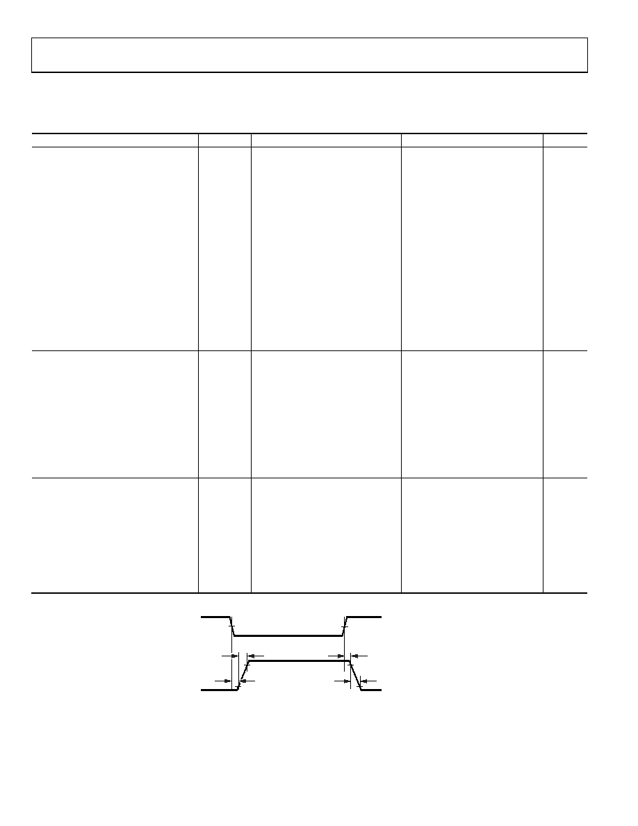
V-DRIVER
INPUT
tRLM, tRMH, tRLH
50%
10%
90%
tPLM, tPMH, tPLH
V-DRIVER
OUTPUT
10%
50%
90%
tFML, tFHM, tFHL
tPML, tPHM, tPHL
10693-
002
Figure 2. Definition of V-Driver Timing Specifications
相關(guān)PDF資料 |
PDF描述 |
|---|---|
| ADG3123BRUZ-REEL7 | IC LEVEL TRANSLATOR 8CH 20-TSSOP |
| ADG3231BRJ-REEL7 | IC SW LLT 1.65/3.6 LV SOT23-6 |
| ADG3232BRJ-REEL7 | IC SW LLT 1.65/3.6 LV SOT23-8 |
| ADG3233BRM-REEL | IC SW LLT 1.65/3.6V BYPASS 8MSOP |
| ADG3241BKSZ-REEL7 | IC SW BUS 2.5-3.3V 1BIT SC70-6 |
相關(guān)代理商/技術(shù)參數(shù) |
參數(shù)描述 |
|---|---|
| ADDI9023BBCZRL | 功能描述:IC VERT DVR 12CH CCD 40CSPBGA RoHS:是 類別:集成電路 (IC) >> 線性 - 視頻處理 系列:- 產(chǎn)品變化通告:Product Discontinuation 07/Mar/2011 標(biāo)準(zhǔn)包裝:3,000 系列:OMNITUNE™ 類型:調(diào)諧器 應(yīng)用:移動電話,手機(jī),視頻顯示器 安裝類型:表面貼裝 封裝/外殼:65-WFBGA 供應(yīng)商設(shè)備封裝:PG-WFSGA-65 包裝:帶卷 (TR) 其它名稱:SP000365064 |
| AD-DIL-SW/04-N | 制造商:Assmann Electronics Inc 功能描述:Switch DIP ON OFF SPST 4 Raised Slide 0.025A 24VDC PC Pins 5000Cycle 2.54mm Thru-Hole 制造商:Assmann Electronics Inc 功能描述:DIP SWITCH HIGH PROFILE 04 CONTACTS |
| AD-DIL-SW/08-N | 制造商:Assmann Electronics Inc 功能描述:Switch DIP ON OFF SPST 8 Raised Slide 0.025A 24VDC PC Pins 5000Cycle 2.54mm Thru-Hole |
| AD-DIO-L/05-180 | 制造商:Assmann Electronics Inc 功能描述: |
| AD-DIO-M/03 | 制造商:Assmann 功能描述:3w MiniDin assembly version plug |
發(fā)布緊急采購,3分鐘左右您將得到回復(fù)。