- 您現(xiàn)在的位置:買賣IC網(wǎng) > PDF目錄384090 > ADC1215S065HN (NXP Semiconductors N.V.) Single 12-bit ADC 65 Msps with Input Buffer CMOS or LVDS DDR digital outputs PDF資料下載
參數(shù)資料
| 型號: | ADC1215S065HN |
| 廠商: | NXP Semiconductors N.V. |
| 元件分類: | 外設(shè)及接口 |
| 英文描述: | Single 12-bit ADC 65 Msps with Input Buffer CMOS or LVDS DDR digital outputs |
| 封裝: | ADC1215S065HN/C1<SOT618-6 (HVQFN40)|<<http://www.nxp.com/packages/SOT618-6.html<1<Always Pb-free,;ADC1215S065HN/C1<SOT618-6 (HVQFN40)|<<http://www.nxp.com/packages/SOT618 |
| 文件頁數(shù): | 24/42頁 |
| 文件大小: | 292K |
| 代理商: | ADC1215S065HN |
第1頁第2頁第3頁第4頁第5頁第6頁第7頁第8頁第9頁第10頁第11頁第12頁第13頁第14頁第15頁第16頁第17頁第18頁第19頁第20頁第21頁第22頁第23頁當(dāng)前第24頁第25頁第26頁第27頁第28頁第29頁第30頁第31頁第32頁第33頁第34頁第35頁第36頁第37頁第38頁第39頁第40頁第41頁第42頁
ADC1215S_SER
All information provided in this document is subject to legal disclaimers.
NXP B.V. 2011. All rights reserved.
Product data sheet
Rev. 2 — 13 January 2011
24 of 42
NXP Semiconductors
ADC1215S series
Single 12-bit ADC; input buffer; CMOS or LVDS DDR digital output
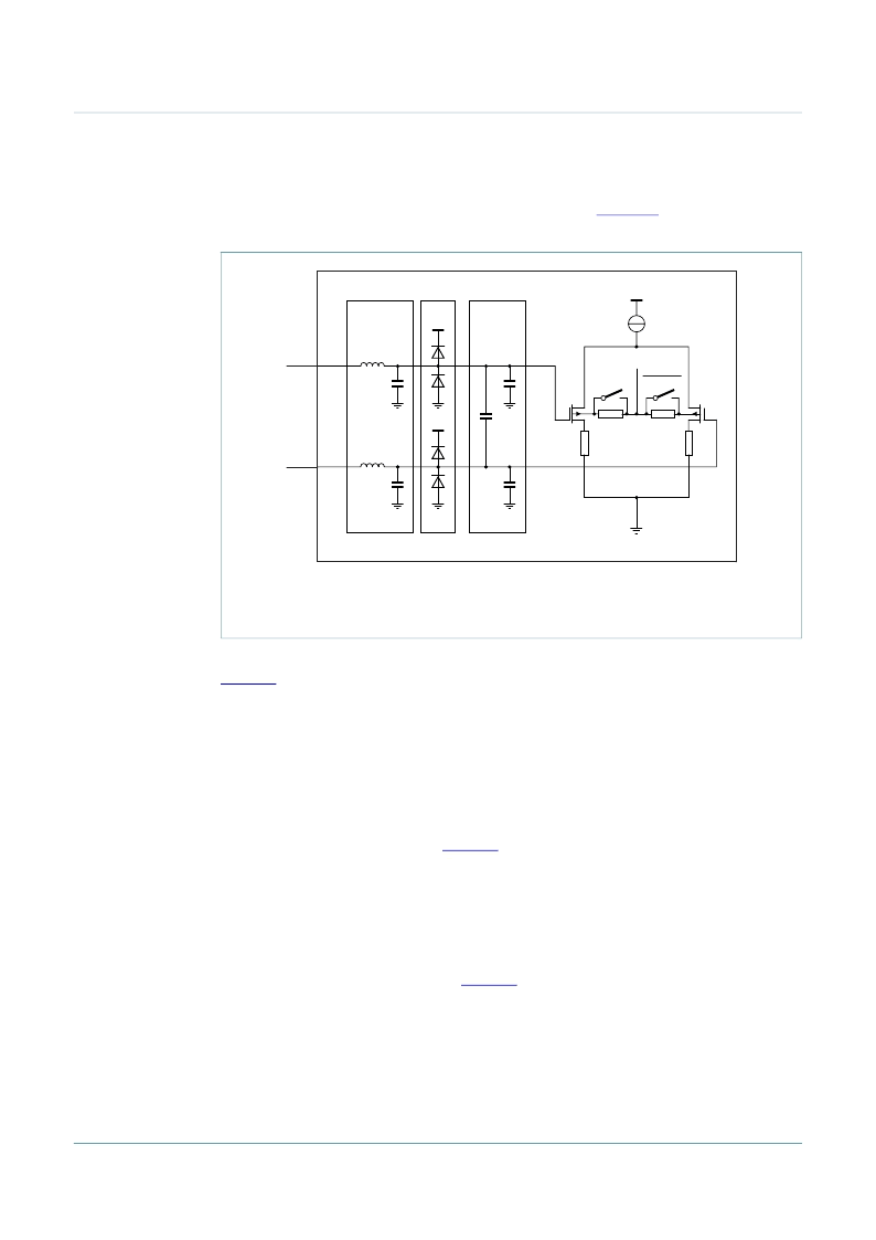
11.4.2
Equivalent input circuit
The equivalent circuit of the input clock buffer is shown in
Figure 24
. The common-mode
voltage of the differential input stage is set via internal 5 k
Ω
resistors.
Single-ended or differential clock inputs can be selected via the SPI interface (see
Table 20
). If single-ended is enabled, the input pin (CLKM or CLKP) is selected via control
bit SE_SEL.
If single-ended is implemented without setting bit SE_SEL to the appropriate value, the
unused pin should be connected to ground via a capacitor.
11.4.3
Duty cycle stabilizer
The duty cycle stabilizer can improve the overall performances of the ADC by
compensating the duty cycle of the input clock signal. When the duty cycle stabilizer is
active (bit DCS_EN = logic 1; see
Table 20
), the circuit can handle signals with duty
cycles of between 30 % and 70 % (typical). When the duty cycle stabilizer is disabled
(DCS_EN = logic 0), the input clock signal should have a duty cycle of between 45 % and
55 %.
11.4.4
Clock input divider
The ADC1215S contains an input clock divider that divides the incoming clock by a factor
of 2 (when bit CLKDIV = logic 1; see
Table 20
). This feature allows the user to deliver a
higher clock frequency with better jitter performance, leading to a better SNR result once
acquisition has been performed.
V
cm(clk)
= common-mode voltage of the differential input stage.
Fig 24. Equivalent input circuit
CLKP
CLKM
005aaa056
Package
ESD
Parasitics
5 k
Ω
5 k
Ω
V
cm(clk)
SE_SEL
SE_SEL
相關(guān)PDF資料 |
PDF描述 |
|---|---|
| ADC1215S065HN | Single 12-bit ADC 65 Msps with Input Buffer CMOS or LVDS DDR digital outputs |
| ADC1215S080HN | Single 12-bit ADC 80 Msps with Input Buffer CMOS or LVDS DDR digital outputs |
| ADC1215S105HN | Single 12-bit ADC 105 Msps with Input Buffer CMOS or LVDS DDR digital outputs |
| ADC1215S125HN | Single 12-bit ADC 125 Msps with Input Buffer CMOS or LVDS DDR digital outputs |
| ADC1415S065F1 | |
相關(guān)代理商/技術(shù)參數(shù) |
參數(shù)描述 |
|---|---|
| ADC1215S065HN/C1 | 制造商:PHILIPS 制造商全稱:NXP Semiconductors 功能描述:Single 12-bit ADC; 65 Msps, 80 Msps, 105 Msps or 125 Msps with input buffer; CMOS or LVDS DDR digital outputs |
| ADC1215S065HN/C1,5 | 功能描述:模數(shù)轉(zhuǎn)換器 - ADC SGL 12BIT ADC 65MSPS IN BUF CMOS/LVDS DDR RoHS:否 制造商:Texas Instruments 通道數(shù)量:2 結(jié)構(gòu):Sigma-Delta 轉(zhuǎn)換速率:125 SPs to 8 KSPs 分辨率:24 bit 輸入類型:Differential 信噪比:107 dB 接口類型:SPI 工作電源電壓:1.7 V to 3.6 V, 2.7 V to 5.25 V 最大工作溫度:+ 85 C 安裝風(fēng)格:SMD/SMT 封裝 / 箱體:VQFN-32 |
| ADC1215S065HN-C1 | 制造商:Integrated Device Technology Inc 功能描述:HVQFN40 - Bulk |
| ADC1215S065HN-C18 | 制造商:Integrated Device Technology Inc 功能描述:HVQFN40 - Tape and Reel |
發(fā)布緊急采購,3分鐘左右您將得到回復(fù)。