- 您現(xiàn)在的位置:買賣IC網(wǎng) > PDF目錄375249 > AD9865-EB (Analog Devices, Inc.) Broadband Modem Mixed-Signal Front End PDF資料下載
參數(shù)資料
| 型號: | AD9865-EB |
| 廠商: | Analog Devices, Inc. |
| 英文描述: | Broadband Modem Mixed-Signal Front End |
| 中文描述: | 寬帶調(diào)制解調(diào)器混合信號前端 |
| 文件頁數(shù): | 31/48頁 |
| 文件大小: | 1672K |
| 代理商: | AD9865-EB |
第1頁第2頁第3頁第4頁第5頁第6頁第7頁第8頁第9頁第10頁第11頁第12頁第13頁第14頁第15頁第16頁第17頁第18頁第19頁第20頁第21頁第22頁第23頁第24頁第25頁第26頁第27頁第28頁第29頁第30頁當(dāng)前第31頁第32頁第33頁第34頁第35頁第36頁第37頁第38頁第39頁第40頁第41頁第42頁第43頁第44頁第45頁第46頁第47頁第48頁
AD9865
outputs left open for optimum linearity performance. The
transformer
1
should be specified to handle the dc standing
current, I
BIAS
, drawn by the IAMP. Also, because I
BIAS
remains
signal independent, a series resistor (not shown) can be inserted
between AVDD and the transformer’s center-tap to reduce the
IAMP’s common-mode voltage, V
CM
, and reduce the power
dissipation on the IC. The V
CM
bias should not exceed 5.0 V and
the power dissipated in the IAMP alone is as follows:
Rev. A | Page 31 of 48
P
IAMP
=
2 × (
N
+
G
) ×
I
×
V
CM
(2)
TxDAC
4
IOUTN–
IOUTN+
IOUTG–
IOUTG+
I
I
0 TO –7.5dB
0 TO –12dB
IAMP
R
R
R
SET
0.1
μ
F
R
L
AVDD
0.1
μ
F
I
BIAS
= 2
×
(N+G)
×
1
IOUT
PK
T:1
IOUT
PK
= (N+G)
×
1
P_OUT
PK
= (IOUT
PK
)
2
×
T
2
×
R
L
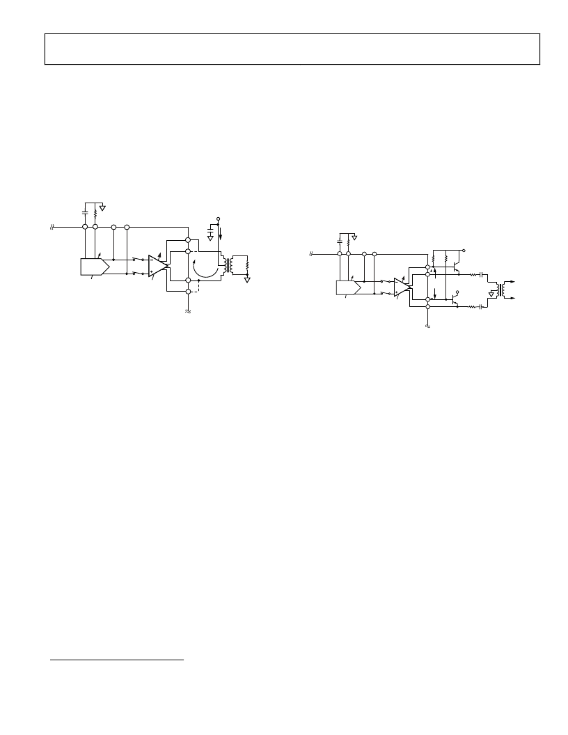
Figure 64. Current-Mode Operation
A step-down transformer
1
with a turn ratio, T, can be used to
increase the output power, P_OUT, delivered to the load. This
causes the output load, R
L
, to be reflected back to the IAMP’s
differential output by T
2
, resulting in a larger differential voltage
swing seen at the IAMP’s output. For example, the IAMP can
deliver 24 dBm of peak power to a 50 load, if a 1.41:1 step-
down transformer is used. This results in 5 V p-p voltage swings
appearing at IOUTN+ and IOUTN pins. Figure 42 shows how
the third order intercept point, OIP3, of the IAMP varies as a
function of common-mode voltage over a 2.5 MHz to 20.0 MHz
span with a 2-tone signal having a peak power of approximately
24 dBm with IOUT
PK
= 50 mA.
For applications requiring an IOUT
PK
exceeding 50 mA, set the
secondary’s path to deliver the additional current to the load.
IOUTG+ and IOUTN+ should be shorted as well as IOUTG
and IOUTN. If IOUT
PK
represents the peak current to be
delivered to the load, then the current gain in the secondary
path, G, can be set by the following equation:
G
=
IOUT
PK
/12.5 4
(3)
The linearity performance becomes limited by the secondary
mirror path’s distortion.
1
The B6080 and BX6090 transformers from Pulse Engineering are worthy of
consideration for current and voltage modes.
IAMP VOLTAGE-MODE OPERATION
The voltage-mode configuration is shown in Figure 65. This
configuration is suited for applications having a poorly defined
load that can vary over a considerable range. A low impedance
voltage driver can be realized with the addition of two external
RF bipolar npn transistors (Phillips PBR951) and resistors. In
this configuration, the current mirrors in the primary path
(IOUTN outputs) feed into scaling resistors, R, generating a
differential voltage into the bases of the npn transistors. These
transistors are configured as source followers with the secon-
dary path current mirrors appearing at IOUTG+ and IOUTG
providing a signal-dependent bias current. Note that the
IOUTP outputs
must
remain open for proper operation.
4
IOUTN–
IOUTN+
IOUTG–
IOUTG+
I
I
0 TO –7.5dB
0 TO –12dB
R
R
R
SET
0.1
μ
F
TO LOAD
AVDD
IOUT
PK
R
R
AVDD
R
S
0.1
μ
F
R
S
0.1
μ
F
DUAL NPN
PHILLIPS PBR951
IAMP
TxDAC
Figure 65. Voltage-Mode Operation
The peak differential voltage signal developed across the npn’s
bases is as follows:
VOUT
PK
=
R
× (
N
×
I
)
(4)
where:
N
is the gain setting of the primary mirror.
I
is the standing current of the TxDAC defined in Equation 1.
The common-mode bias voltage seen at IOUTN+ and IOUTN
is approximately AVDD VOUT
PK
, while the common-mode
voltage seen at IOUTG+ and IOUTG is approximately the
npn’s V
BE
drop below this level (AVDD VOUT
PK
0.65). In
the voltage-mode configuration, the total power dissipated
within the IAMP is as follows :
P
IAMP
= 2 ×
I
× {(
AVDD
VOUT
PK
) ×
N
+ (
AVDD
VOUT
PK
0.65) ×
G}
(5)
The emitters of the npn transistors are ac-coupled to the trans-
former
1
via a 0.1 μF blocking capacitor and series resistor of 1
to 2 . Note that protection diodes are not shown for clarity
purposes, but should be considered if interfacing to a power or
phone line.
The amount of standing and signal-dependent current used to
bias the npn transistors depends on the peak current, IOUT
PK
,
required by the load. If the load is variable, determine the worst
case, IOUT
PK
, and add 3 mA of margin to ensure that the npn
transistors remain in the active region during peak load
相關(guān)PDF資料 |
PDF描述 |
|---|---|
| AD9865BCP | Broadband Modem Mixed-Signal Front End |
| AD9865BCPRL | Broadband Modem Mixed-Signal Front End |
| AD9865BCPZ1 | Broadband Modem Mixed-Signal Front End |
| AD9865BCPZRL1 | Broadband Modem Mixed-Signal Front End |
| AD9865CHIPS | Broadband Modem Mixed-Signal Front End |
相關(guān)代理商/技術(shù)參數(shù) |
參數(shù)描述 |
|---|---|
| AD9866 | 制造商:AD 制造商全稱:Analog Devices 功能描述:Broadband Modem Mixed-Signal Front End |
| AD9866BCP | 制造商:Analog Devices 功能描述:Mixed Signal Front End 64-Pin LFCSP EP 制造商:Analog Devices 功能描述:12BIT MIXED SIGNAL CONVERTER 9866 |
| AD9866BCPRL | 制造商:Analog Devices 功能描述:Mixed Signal Front End 64-Pin LFCSP EP T/R |
| AD9866BCPZ | 功能描述:IC PROCESSOR FRONT END 64LFCSP RoHS:是 類別:RF/IF 和 RFID >> RF 前端 (LNA + PA) 系列:- 產(chǎn)品培訓(xùn)模塊:Lead (SnPb) Finish for COTS Obsolescence Mitigation Program 標(biāo)準(zhǔn)包裝:250 系列:- RF 型:GPS 頻率:1575.42MHz 特點(diǎn):- 封裝/外殼:48-TQFP 裸露焊盤 供應(yīng)商設(shè)備封裝:48-TQFP 裸露焊盤(7x7) 包裝:托盤 |
| AD9866BCPZRL | 功能描述:IC PROCESSOR FRONT END 64LFCSP RoHS:是 類別:RF/IF 和 RFID >> RF 前端 (LNA + PA) 系列:- 產(chǎn)品培訓(xùn)模塊:Lead (SnPb) Finish for COTS Obsolescence Mitigation Program 標(biāo)準(zhǔn)包裝:250 系列:- RF 型:GPS 頻率:1575.42MHz 特點(diǎn):- 封裝/外殼:48-TQFP 裸露焊盤 供應(yīng)商設(shè)備封裝:48-TQFP 裸露焊盤(7x7) 包裝:托盤 |
發(fā)布緊急采購,3分鐘左右您將得到回復(fù)。