- 您現(xiàn)在的位置:買賣IC網(wǎng) > PDF目錄373959 > AD9200JST (ANALOG DEVICES INC) Complete 10-Bit, 20 MSPS, 80 mW CMOS A/D Converter PDF資料下載
參數(shù)資料
| 型號(hào): | AD9200JST |
| 廠商: | ANALOG DEVICES INC |
| 元件分類: | ADC |
| 英文描述: | Complete 10-Bit, 20 MSPS, 80 mW CMOS A/D Converter |
| 中文描述: | 1-CH 10-BIT PROPRIETARY METHOD ADC, PARALLEL ACCESS, PQFP48 |
| 封裝: | PLASTIC, LQFP-48 |
| 文件頁數(shù): | 13/24頁 |
| 文件大?。?/td> | 338K |
| 代理商: | AD9200JST |
AD9200
–13–
REV. E
The input capacitor should be sized to allow sufficient acquisi-
tion time of the clamp voltage at AIN within the CLAMP inter-
val, but also be sized to minimize droop between clamping
intervals. Specifically, the acquisition time when the switch is
closed will equal:
T
ACQ
=
R
IN
C
IN
lnV
C
V
E
where
V
C
is the voltage change required across
C
IN
, and
V
E
is
the error voltage. V
C
is calculated by taking the difference be-
tween the initial input dc level at the start of the clamp interval
and the clamp voltage supplied at CLAMPIN. V
E
is a system-
dependent parameter, and equals the maximum tolerable devia-
tion from V
C
. For example, if a 2-volt input level needs to be
clamped to 1 volt at the AD9200’s input within 10 millivolts,
then V
C
equals 2 – 1 or 1 volt, and V
E
equals 10 mV. Note that
once the proper clamp level is attained at the input, only a very
small voltage change will be required to correct for droop.
The voltage droop is calculated with the following equation:
dV
=
I
BIAS
C
IN
t
( )
where
t
= time between clamping intervals.
The bias current of the AD9200 will depend on the sampling
rate, F
S
. The switched capacitor input AIN appears resistive
over time, with an input resistance equal to 1/C
S
F
S
. Given a
sampling rate of 20 MSPS and an input capacitance of 1 pF, the
input resistance is 50 k
. This input resistance is equivalently
terminated at the midscale voltage of the input range. The worst
case bias current will thus result when the input signal is at the
extremes of the input range, that is, the furthest distance from
the midscale voltage level. For a 1-volt input range, the maxi-
mum bias current will be
±
0.5 volts divided by 50 k
, which is
±
10
μ
A.
If droop is a critical parameter, then the minimum value of C
IN
should be calculated first based on the droop requirement.
Acquisition time—the width of the CLAMP pulse—can be
adjusted accordingly once the minimum capacitor value is cho-
sen. A tradeoff will often need to be made between droop and
acquisition time, or error voltage V
E
.
Clamp Circuit Example
A single supply video amplifier outputs a level-shifted video
signal between 2 and 3 volts with the following parameters:
horizontal period = 63.56
μ
s,
horizontal sync interval = 10.9
μ
s,
horizontal sync pulse = 4.7
μ
s,
sync amplitude = 0.3 volts,
video amplitude of 0.7 volts,
reference black level = 2.3 volts
The video signal must be dc restored from a 2- to 3-volt range
down to a 1- to 2-volt range. Configuring the AD9200 for a
one volt input span with an input range from 1 to 2 volts (see
Figure 24), the CLAMPIN voltage can be set to 1 volt with an
external voltage or by direct connection to REFBS. The CLAMP
pulse may be applied during the SYNC pulse, or during the
back porch to truncate the SYNC below the AD9200’s mini-
mum input voltage. With a C
IN
= 1
μ
F, and R
IN
= 20
, the
acquisition time needed to set the input dc level to one volt
with 1 mV accuracy is about 140
μ
s, assuming a full 1 volt V
C
.
With a 1
μ
F input coupling capacitor, the droop across one
horizontal can be calculated:
I
BIAS
= 10
μ
A, and t = 63.5
μ
s, so dV = 0.635 mV, which is less
than one LSB.
After the input capacitor is initially charged, the clamp pulse-
width only needs to be wide enough to correct small voltage
errors such as the droop. The fine scale settling characteristics
of the clamp circuitry are shown in Table II.
Depending on the required accuracy, a CLAMP pulsewidth of
1
μ
s–3
μ
s should work in most applications. The OFFSET val-
ues ignore the contribution of offset from the clamp amplifier;
they simply compare the output code with a “final value” mea-
sured with a much longer CLAMP pulse duration.
Table II.
CLAMP
10
μ
s
5
μ
s
4
μ
s
3
μ
s
2
μ
s
1
μ
s
OFFSET
<1 LSB
5 LSBs
7 LSBs
11 LSBs
19 LSBs
42 LSBs
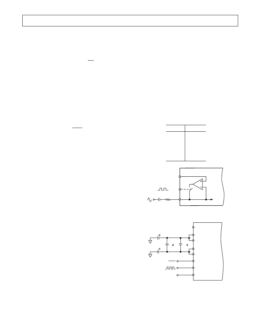
CLAMP IN
AD9200
CLAMP
AIN
CIN
RIN
TO
SHA
SW1
Figure 24a. Clamp Operation
0.1 F
10 F
AIN
REFTF
REFBS
MODE
AD9200
REFTS
0.1 F
REFBF
CLAMP
CLAMPIN
AVDD
2
SHORT TO REFBS
OR EXTERNAL DC
0.1 F
Figure 24b. Video Clamp Circuit
相關(guān)PDF資料 |
PDF描述 |
|---|---|
| AD9200JSTRL | Complete 10-Bit, 20 MSPS, 80 mW CMOS A/D Converter |
| AD9201 | Dual Channel, 20 MHz 10-Bit Resolution CMOS ADC |
| AD9201-EVAL | Dual Channel, 20 MHz 10-Bit Resolution CMOS ADC |
| AD9201ARS | Dual Channel, 20 MHz 10-Bit Resolution CMOS ADC |
| AD9201EVALBOARD | Octal I2C 16-Bit Rail-to-Rail DACs in 16-Lead SSOP; Package: SSOP; No of Pins: 16; Temperature Range: -40°C to +85°C |
相關(guān)代理商/技術(shù)參數(shù) |
參數(shù)描述 |
|---|---|
| AD9200JSTRL | 制造商:Rochester Electronics LLC 功能描述:- Tape and Reel 制造商:Analog Devices 功能描述: |
| AD9200JSTZ | 制造商:Rochester Electronics LLC 功能描述:- Bulk 制造商:Analog Devices 功能描述: |
| AD9200KST | 制造商:Rochester Electronics LLC 功能描述:10-BIT 20 MSPS, 80 MW CMOS A/D CONVERTER - Tape and Reel 制造商:Analog Devices 功能描述: |
| AD9200KSTRL | 制造商:Rochester Electronics LLC 功能描述:- Tape and Reel 制造商:Analog Devices 功能描述: |
| AD9200KSTZ | 制造商:Analog Devices 功能描述:ADC SGL PIPELINED 20MSPS 10-BIT PARALLEL 48LQFP - Trays |
發(fā)布緊急采購,3分鐘左右您將得到回復(fù)。