- 您現(xiàn)在的位置:買賣IC網(wǎng) > PDF目錄373959 > AD9101SE (ANALOG DEVICES INC) 125 MSPS Monolithic Sampling Amplifier PDF資料下載
參數(shù)資料
| 型號: | AD9101SE |
| 廠商: | ANALOG DEVICES INC |
| 元件分類: | 運動控制電子 |
| 英文描述: | 125 MSPS Monolithic Sampling Amplifier |
| 中文描述: | TRACK AND HOLD AMPLIFIER, CQCC20 |
| 封裝: | CERAMIC, LCC-20 |
| 文件頁數(shù): | 3/12頁 |
| 文件大小: | 247K |
| 代理商: | AD9101SE |
NOT ES
1
If the analog input exceeds
±
300 mV, the clock levels should be shifted as shown in the T heory of Operation section entitled “Driving the Encode Clock.”
2
T ime to recover within rated error band from 160% overdrive.
3
Sampling bandwidth is defined as the –3 dB frequency response of the input sampler to the hold capacitor when operating in the sampling mode. It is greater than
tracking bandwidth because it does not include the bandwidth of the output amplifier.
4
Hold mode noise is proportional to the length of time a signal is held. For example, if the hold time (t
H
) is 20 ns, the accumulated noise is typically 3
μ
V
(150 mV/s
×
20 ns). T his value must be combined with the track mode noise to obtain total noise.
5
T otal energy of worst case track-to-hold or hold-to-track glitch.
Specifications subject to change without notice.
–3–
REV. 0
AD9101
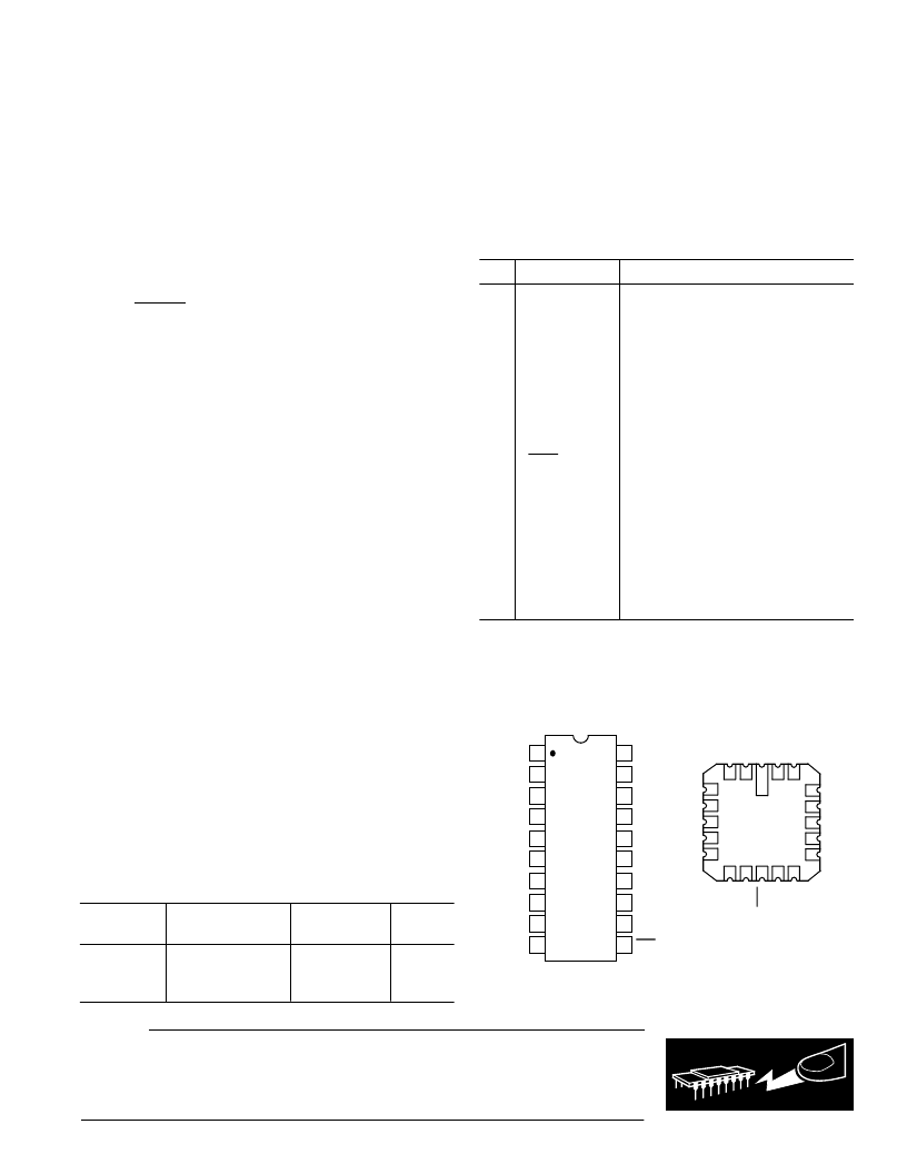
20-Pin SOIC
RTN
RTN
C
B+
CLK
NC
V
IN
V
OUT
GND
CLK
GND
GND
1
2
3
4
5
6
7
8
9
10
20
19
18
17
16
15
14
13
12
11
TOP VIEW
(Not to Scale)
AD9101
+V
S
+V
S
+V
S
+V
S
C
B–
–V
S
–V
S
–V
S
–V
S
20-Contact Ceramic LCC
1
2
3
4
5
6
7
8
9
10
11
12
13
14
15
16
17
18
19 20
BOTTOM VIEW
R
R
GND
GND
+V
S
C
B
C
–V
S
–V
S
NC
V
IN
V
O
GND
C
C
B
+V
S
+V
S
–
S
–
S
+
S
PIN CONFIGURAT IONS
ABSOLUT E MAX IMUM RAT INGS
1
Supply Voltage (+V
S
) . . . . . . . . . . . . . . . . . . . . –0.5 V to +6 V
Supply Voltage (–V
S
) . . . . . . . . . . . . . . . . . . . . –6 V to +0.5 V
Analog Input Voltage . . . . . . . . . . . . . . . . . . . . . . . . . . . .
±
5 V
CLOCK /
CLOCK
Input . . . . . . . . . . . . . . . . . –5 V to +0.5 V
Continuous Output Current
4
. . . . . . . . . . . . . . . . . . . . 70 mA
Storage T emperature . . . . . . . . . . . . . . . . . . –65
°
C to +150
°
C
Operating T emperature Range
AE, AR . . . . . . . . . . . . . . . . . . . . . . . . . . . . –40
°
C to +85
°
C
SE . . . . . . . . . . . . . . . . . . . . . . . . . . . . . . –55
°
C to +125
°
C
Junction T emperature (Ceramic)
2
. . . . . . . . . . . . . . . +175
°
C
Junction T emperature (Plastic)
2
. . . . . . . . . . . . . . . . +150
°
C
Soldering T emperature (1 minute)
3
. . . . . . . . . . . . . . +220
°
C
NOT ES
1
Absolute maximum ratings are limiting values to be applied individually, and
beyond which the serviceability of the circuit may be impaired. Functional
operability is not necessarily implied. Exposure to absolute maximum rating
conditions for an extended period of time may affect device reliability.
2
T ypical thermal impedances (no air flow, soldered to PC board) are as follows:
Ceramic LCC:
θ
JA
= 48
°
C/W;
θ
JC
= 9.9
°
C/W; Plastic SOIC:
θ
JA
= 54
°
C/W;
θ
= 7.3
°
C/W.
3
For surface mount devices, mounted by vapor phase soldering. Prior to vapor phase
soldering, plastic units should receive a minimum eight hour bakeout at 110
°
C to
drive off any moisture absorbed in plastic during shipping or storage. T hrough-hole
devices can be soldered at +300
°
C for 10 seconds.
4
Output is short circuit protected to ground. Continuous short circuit may affect
device reliability.
Pin Description
Pin
Description
Connection
1
2
3
4
5
6
7
8
9
10
11
12
13
14
15
16
17
18
19
20
RT N
RT N
C
B+
+V
S
+V
S
GND
GND
+V
S
+V
S
CLK
CLK
–V
S
–V
S
N/C
V
IN
GND
–V
S
–V
S
C
B–
V
OUT
Gain Set Resistor Return*
Gain Set Resistor Return*
Bootstrap Capacitor (Positive Bias)
+5 V Power Supply (Analog)
+5 V Power Supply (Analog)
Hold Capacitor Ground
Hold Capacitor Ground
+5 V Power Supply (Digital)
+5 V Power Supply (Digital)
T rue ECL T /H Clock
Complement ECL T /H Clock
–5.2 V Power Supply (Digital)
–5.2 V Power Supply (Digital)
No Connection
Analog Signal Input
Ground (Signal Return)
–5.2 V Power Supply (Analog)
–5.2 V Power Supply (Analog)
Bootstrap Capacitor (Negative Bias)
Analog Signal Output
*See “Matching the AD9101 to A/D Encoders.” Both pins should either be
grounded or connected to voltage source for offset.
WARNING!
ESD SENSITIVE DEVICE
C AUT ION
ESD (electrostatic discharge) sensitive device. Electrostatic charges as high as 4000 V readily
accumulate on the human body and test equipment and can discharge without detection.
Although the AD9101 features proprietary ESD protection circuitry, permanent damage may
occur on devices subjected to high energy electrostatic discharges. T herefore, proper ESD
precautions are recommended to avoid performance degradation or loss of functionality.
E X PLANAT ION OF T E ST LE VE LS
T est Level
I
– 100% production tested.
II
– 100% production tested at +25
°
C, and sample tested at
specified temperatures.
III – Periodically sample tested.
IV – Parameter is guaranteed by design and characterization
testing.
V
– Parameter is a typical value only.
VI – All devices are 100% production tested at +25
°
C. 100%
production tested at temperature extremes for extended
temperature devices; sample tested at temperature
extremes for commercial/industrial devices.
ORDE RING INFORMAT ION
T emperature
Range
Package
Description
Package
Option
Model
AD9101AR
AD9101AE
AD9101SE
–40
°
C to +85
°
C
–40
°
C to +85
°
C
–55
°
C to +125
°
C
Plastic SOIC
LCC
LCC
R-20
E-20A
E-20A
相關PDF資料 |
PDF描述 |
|---|---|
| AD9101 | 125 MSPS Monolithic Sampling Amplifier(125MSPS單片采樣放大器) |
| AD9200KST | Complete 10-Bit, 20 MSPS, 80 mW CMOS A/D Converter |
| AD9200LQFP-EVAL | Complete 10-Bit, 20 MSPS, 80 mW CMOS A/D Converter |
| AD9200JRSRL | Complete 10-Bit, 20 MSPS, 80 mW CMOS A/D Converter |
| AD9200ARSRL | Complete 10-Bit, 20 MSPS, 80 mW CMOS A/D Converter |
相關代理商/技術參數(shù) |
參數(shù)描述 |
|---|---|
| AD9102 | 制造商:AD 制造商全稱:Analog Devices 功能描述:Low Power, 14-Bit, 180 MSPS, Digital-to-Analog Converter and Waveform Generator |
| AD91020 | 制造商:Analog Devices 功能描述: |
| AD9102BCPZ | 功能描述:數(shù)模轉(zhuǎn)換器- DAC 14 bit Single Channel DAC RoHS:否 制造商:Texas Instruments 轉(zhuǎn)換器數(shù)量:1 DAC 輸出端數(shù)量:1 轉(zhuǎn)換速率:2 MSPs 分辨率:16 bit 接口類型:QSPI, SPI, Serial (3-Wire, Microwire) 穩(wěn)定時間:1 us 最大工作溫度:+ 85 C 安裝風格:SMD/SMT 封裝 / 箱體:SOIC-14 封裝:Tube |
| AD9102BCPZRL7 | 功能描述:數(shù)模轉(zhuǎn)換器- DAC Low Power 14-Bit 180MSPS RoHS:否 制造商:Analog Devices 轉(zhuǎn)換器數(shù)量:4 DAC 輸出端數(shù)量:4 轉(zhuǎn)換速率: 分辨率:12 bit 接口類型:Serial (I2C) 穩(wěn)定時間: 最大工作溫度:+ 105 C 安裝風格: 封裝 / 箱體:TSSOP 封裝:Reel |
| AD9102-EBZ | 功能描述:數(shù)據(jù)轉(zhuǎn)換 IC 開發(fā)工具 14 bit Single Channel DAC RoHS:否 制造商:Texas Instruments 產(chǎn)品:Demonstration Kits 類型:ADC 工具用于評估:ADS130E08 接口類型:SPI 工作電源電壓:- 6 V to + 6 V |
發(fā)布緊急采購,3分鐘左右您將得到回復。