- 您現(xiàn)在的位置:買賣IC網(wǎng) > PDF目錄375243 > AD8315 (Analog Devices, Inc.) 50 dB GSM PA Controller PDF資料下載
參數(shù)資料
| 型號: | AD8315 |
| 廠商: | Analog Devices, Inc. |
| 英文描述: | 50 dB GSM PA Controller |
| 中文描述: | 50分貝的GSM PA控制器 |
| 文件頁數(shù): | 15/20頁 |
| 文件大?。?/td> | 1787K |
| 代理商: | AD8315 |
REV. B
AD8315
–15–
Using the Chip Scale Package
On the underside of the chip scale package, there is an exposed
paddle. This paddle is internally connected to the chip’s ground.
There is no thermal requirement to solder the paddle down to the
printed circuit board’s ground plane. However, soldering down
the paddle has been shown to increase the stability over frequency
of the AD8315 ACP’s response at low input power levels (i.e., at
around –45 dBm) in the DCS and PCS bands
.
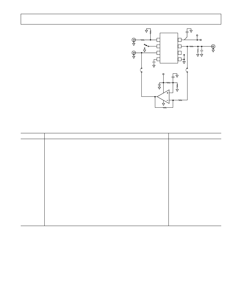
Evaluation Board
Figure 11 shows the schematic of the AD8315 MSOP evaluation
board. The layout and silkscreen of the component side are
shown in Figures 12 and 13. An evaluation board is also available
for the LFCSP package (for exact part numbers, see Ordering
Guide). Apart from the slightly smaller device footprint, the
LFCSP evaluation board is identical to the MSOP board. The
board is powered by a single supply in the range, 2.7 V to 5.5 V.
The power supply is decoupled by a single 0.1 F capacitor.
Table II details the various configuration options of the
evaluation board.
V
POS
R3
0
J2
VAPC
R4
(OPEN)
C2
(OPEN)
NC = NO CONNECT
RFIN
ENBL
VSET
VPOS
VAPC
NC
COMM
FLTR
AD8315
1
2
3
4
5
6
7
8
R2
52.3
C4
(OPEN)
C1
0.1 F
R1
0
J1
LK2
LK1
VPOS
SW1
RFIN
J3
VSET
AD8031
V
POS
R7
C3
0.1 F
R8
10k
C5
0.1 F
R6
R5
10k
16.2k
17.8k
TP1
TP2
Figure 11. Evaluation Board Schematic
Table II. Evaluation Board Configuration Options
Component
Function
Default Condition
TP1, TP2
SW1
Supply and Ground Vector Pins
Device Enable: When in Position A, the ENBL pin is connected to VPOS and
the AD8315 is in operating mode. In Position B, the ENBL pin is grounded
putting the device in power-down mode.
Input Interface: The 52.3
W
resistor in Position R2 combines with the
AD8315’s internal input impedance to give a broadband input impedance
of around 50
W
. A reactive match can be implemented by replacing R2 with
an inductor and R1 (0
W
) with a capacitor. Note that the AD8315’s RF input
is internally ac-coupled.
Output Interface: R4 and C2 can be used to check the response of V
APC
to
capacitive and resistive loading. R3/R4 can be used to reduce the slope of V
APC
.
Power Supply Decoupling: The nominal supply decoupling consists of a
0.1
m
F capacitor.
Filter Capacitor: The response time of V
APC
can be modified by placing a
capacitor between FLTR (Pin 4) and ground.
Measurement Mode: A quasi-measurement mode can be implemented by
installing LK1 and LK2 (connecting an inverted V
APC
to V
SET
) to yield the
nominal relationship between RFIN and V
SET
. In this mode, a large capacitor
(0.01
m
F or greater) must be installed in C4.
Not Applicable
SW1 = A
R1, R2
R2 = 52.3
W
(Size 0603)
R1 = 0
W
(Size 0402)
R3, R4, C2
R4 = C2 = Open (Size 0603)
R3 = 0
W
(Size 0603)
C1 = 0.1
m
F (Size 0603)
C1
C4
C4 = Open (Size 0603)
LK1, LK2
LK1, LK2 = Installed
相關(guān)PDF資料 |
PDF描述 |
|---|---|
| AD8315-EVAL | 50 dB GSM PA Controller |
| AD8315ACP-EVAL | 50 dB GSM PA Controller |
| AD8315ACP-REEL | 50 dB GSM PA Controller |
| AD8315ACP-REEL7 | 50 dB GSM PA Controller |
| AD8315ARM | 50 dB GSM PA Controller |
相關(guān)代理商/技術(shù)參數(shù) |
參數(shù)描述 |
|---|---|
| AD8315_06 | 制造商:AD 制造商全稱:Analog Devices 功能描述:50 dB GSM PA Controller |
| AD8315ACHIPS | 制造商:AD 制造商全稱:Analog Devices 功能描述:50 dB GSM PA Controller |
| AD8315ACP-EVAL | 制造商:Analog Devices 功能描述:EVAL BOARD GSM PA CONTR AD8 |
| AD8315ACP-REEL | 制造商:Analog Devices 功能描述: |
| AD8315ACP-REEL7 | 制造商:Rochester Electronics LLC 功能描述: 制造商:Analog Devices 功能描述: |
發(fā)布緊急采購,3分鐘左右您將得到回復(fù)。