- 您現(xiàn)在的位置:買賣IC網(wǎng) > PDF目錄375243 > AD8315 (Analog Devices, Inc.) 50 dB GSM PA Controller PDF資料下載
參數(shù)資料
| 型號(hào): | AD8315 |
| 廠商: | Analog Devices, Inc. |
| 英文描述: | 50 dB GSM PA Controller |
| 中文描述: | 50分貝的GSM PA控制器 |
| 文件頁(yè)數(shù): | 12/20頁(yè) |
| 文件大小: | 1787K |
| 代理商: | AD8315 |
第1頁(yè)第2頁(yè)第3頁(yè)第4頁(yè)第5頁(yè)第6頁(yè)第7頁(yè)第8頁(yè)第9頁(yè)第10頁(yè)第11頁(yè)當(dāng)前第12頁(yè)第13頁(yè)第14頁(yè)第15頁(yè)第16頁(yè)第17頁(yè)第18頁(yè)第19頁(yè)第20頁(yè)
REV. B
AD8315
–12–
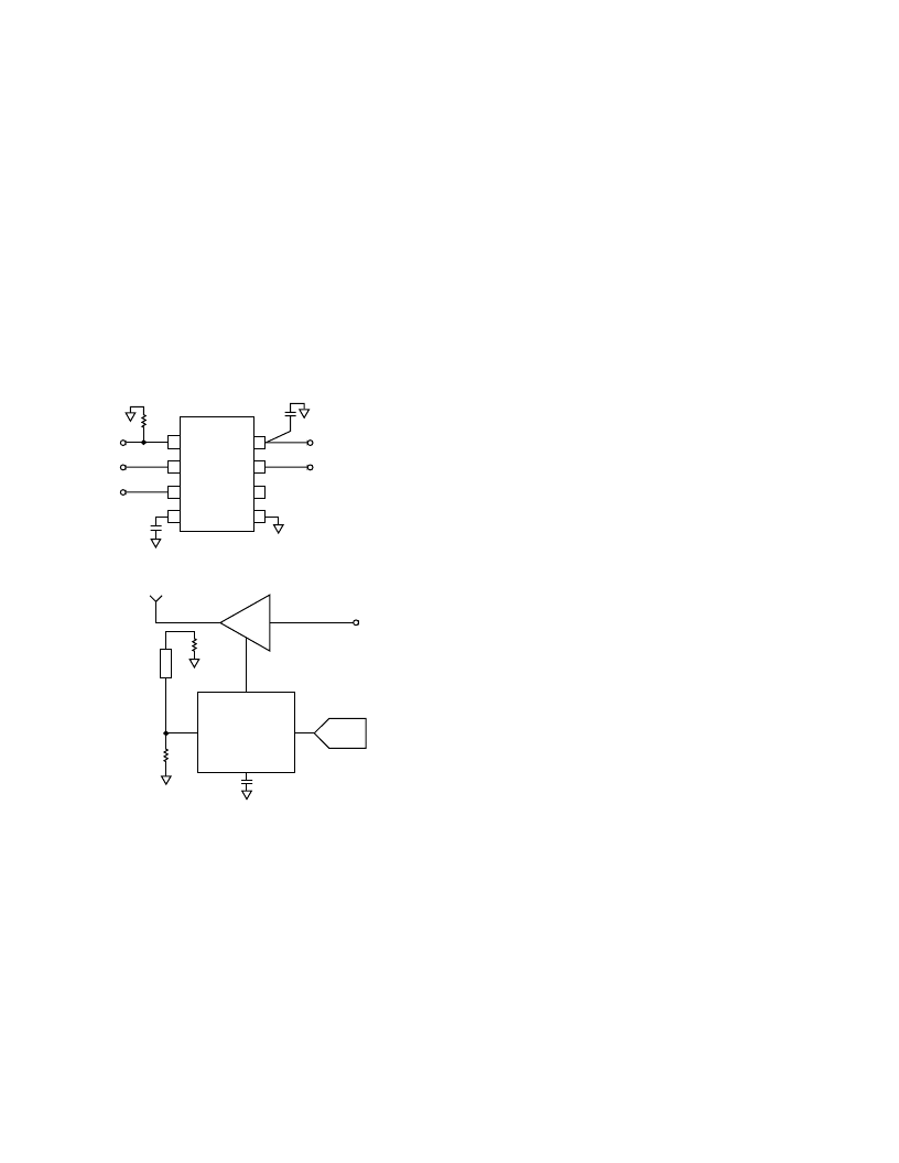
Basic Connections
Figure 6 shows the basic connections for operating the AD8315,
and Figure 7 shows a block diagram of a typical application.
The AD8315 is typically used in the RF power control loop of a
mobile handset.
A supply voltage of 2.7 V to 5.5 V is required for the AD8315.
The supply to the VPOS pin should be decoupled with a low
inductance 0.1
m
F surface-mount ceramic capacitor, close to the
device. The AD8315 has an internal input coupling capacitor.
This negates the need for external ac-coupling. This capacitor,
along with the low frequency input impedance of the device of
approximately 2.8 k
W
, sets the minimum usable input frequency
to around 0.016 GHz. A broadband 50
W
input match is achieved
in this example by connecting a 52.3
W
resistor between RFIN
and ground. A plot of input impedance versus frequency is
shown in TPC 9. Other coupling methods are also possible (see
Input Coupling Options section).
NC = NO CONNECT
RFIN
ENBL
VSET
VPOS
VAPC
NC
COMM
FLTR
AD8315
1
2
3
4
5
6
7
8
R1
52.3
C
FLT
RFIN
+V
S
V
SET
+V
(2.7V TO 5.5V)
+V
APC
C1
0.1 F
Figure 6. Basic Connections
RFIN
VSET
AD8315
VAPC
FLTR
C
FLT
GAIN
CONTROL
VOLTAGE
DAC
POWER
AMP
RFIN
ATTENUATOR
DIRECTIONAL
COUPLER
52.3
Figure 7. Typical Application
In a power control loop, the AD8315 provides both the detector and
controller functions. A sample of the power amplifier’s (PA) output
power is coupled to the RF input of the AD8315, usually via a
directional coupler. In dual mode applications, where there are
two PAs and two directional couplers, the outputs of the directional
couplers can be passively combined (both PAs will never be turned
on simultaneously) before being applied to the AD8315.
A setpoint voltage is applied to VSET from the controlling
source (generally this will be a DAC). Any imbalance between
the RF input level and the level corresponding to the setpoint
voltage will be corrected by the AD8315’s VAPC output that
drives the gain control terminal of the PA. This restores a balance
between the actual power level sensed at the input of the AD8315
and the value determined by the setpoint. This assumes that the gain
control sense of the variable gain element is positive, that is, an
increasing voltage from VAPC will tend to increase gain.
V
APC
can swing from 250 mV to within 100 mV of the supply
rail and can source up to 6 mA. If the control input of the PA
needs to source current, a suitable load resistor can be con-
nected between VAPC and COMM. The output swing and
current sourcing capability of VAPC is shown in TPC 19.
Range on VSET and RFIN
The relationship between the RF input level and the setpoint
voltage follows from the nominal transfer function of the device
(see TPCs 2, 3, 5, and 6). At 0.9 GHz, for example, a voltage of
1 V on VSET indicates a demand for –30 dBV (–17 dBm re 50
W
)
at RFIN. The corresponding power level at the output of the
power amplifier will be greater than this amount due to the
attenuation through the directional coupler.
For setpoint voltages of less than approximately 250 mV, V
APC
will remain unconditionally at its minimum level of approximately
250 mV. This feature can be used to prevent any spurious emissions
during power-up and power-down phases.
Above 250 mV, V
SET
will have a linear control range up to 1.4 V,
corresponding to a dynamic range of 50 dB. This results in a
slope of 23 mV/dB or approximately 43.5 dB/V.
Transient Response
The time domain response of power amplifier control loops,
using any kind of controller, is only partially determined by the
choice of filter which, in the case of the AD8315, has a true
integrator form 1/
sT
as shown in Equation 7, with a time con-
stant given by Equation 8. The large signal step response is
also strongly dependent on the form of the gain-control law.
Nevertheless, some simple rules can be applied. When the filter
capacitor C
FLT
is very large, it will dominate the time domain
response, but the incremental bandwidth of this loop will still
vary as V
APC
traverses the nonlinear gain-control function of the
PA, as sketched in Figure 5. This bandwidth will be highest at
the point where the slope of the tangent drawn on this curve is
greatest—that is, for power outputs near the center of the PA’s
range—and will be much reduced at both the minimum and
the maximum power levels, where the slope of the gain control
curve is lowest, due to its S-shaped form.
Using smaller values of C
FLT
, the loop bandwidth will generally
increase, in inverse proportion to its value. Eventually, however,
a secondary effect will appear, due to the inherent phase lag in
the power amplifier’s control path, some of which may be due to
parasitic or deliberately added capacitance at the VAPC pin.
This results in the characteristic poles in the ac loop equation
moving off the real axis and thus becoming complex (and some-
what resonant). This is a classic aspect of control loop design.
The lowest permissible value of C
FLT
needs to be determined
experimentally for a particular amplifier. For GSM and DCS
power amplifiers, C
FLT
will typically range from 150 pF to 300 pF.
In many cases, some improvement in the worst-case response
time can be achieved by including a small resistance in series
with C
FLT
; this generates an additional zero in the closed-loop
transfer function, that will serve to cancel some of the higher
order poles in the overall loop. A combination of main capacitor
C
FLT
shunted by a second capacitor and resistor in series will
also be useful in minimizing the settling time of the loop.
Mobile Handset Power Control Example
Figure 8 shows a complete power amplifier control circuit for a
dual mode handset. The PF08107B (Hitachi), a dual mode
(GSM, DCS) PA, is driven by a nominal power level of 3 dBm.
相關(guān)PDF資料 |
PDF描述 |
|---|---|
| AD8315-EVAL | 50 dB GSM PA Controller |
| AD8315ACP-EVAL | 50 dB GSM PA Controller |
| AD8315ACP-REEL | 50 dB GSM PA Controller |
| AD8315ACP-REEL7 | 50 dB GSM PA Controller |
| AD8315ARM | 50 dB GSM PA Controller |
相關(guān)代理商/技術(shù)參數(shù) |
參數(shù)描述 |
|---|---|
| AD8315_06 | 制造商:AD 制造商全稱:Analog Devices 功能描述:50 dB GSM PA Controller |
| AD8315ACHIPS | 制造商:AD 制造商全稱:Analog Devices 功能描述:50 dB GSM PA Controller |
| AD8315ACP-EVAL | 制造商:Analog Devices 功能描述:EVAL BOARD GSM PA CONTR AD8 |
| AD8315ACP-REEL | 制造商:Analog Devices 功能描述: |
| AD8315ACP-REEL7 | 制造商:Rochester Electronics LLC 功能描述: 制造商:Analog Devices 功能描述: |
發(fā)布緊急采購(gòu),3分鐘左右您將得到回復(fù)。