- 您現(xiàn)在的位置:買賣IC網(wǎng) > PDF目錄375243 > AD8310ARM-REEL7 (ANALOG DEVICES INC) Fast, Voltage-Out DC-440 MHz 95 dB Logarithmic Amplifier PDF資料下載
參數(shù)資料
| 型號(hào): | AD8310ARM-REEL7 |
| 廠商: | ANALOG DEVICES INC |
| 元件分類: | 運(yùn)動(dòng)控制電子 |
| 英文描述: | Fast, Voltage-Out DC-440 MHz 95 dB Logarithmic Amplifier |
| 中文描述: | LOG OR ANTILOG AMPLIFIER, 440 MHz BAND WIDTH, PDSO8 |
| 封裝: | MO-187AA, MSOP-8 |
| 文件頁(yè)數(shù): | 12/16頁(yè) |
| 文件大?。?/td> | 323K |
| 代理商: | AD8310ARM-REEL7 |
第1頁(yè)第2頁(yè)第3頁(yè)第4頁(yè)第5頁(yè)第6頁(yè)第7頁(yè)第8頁(yè)第9頁(yè)第10頁(yè)第11頁(yè)當(dāng)前第12頁(yè)第13頁(yè)第14頁(yè)第15頁(yè)第16頁(yè)
AD8310
–12–
REV. A
Table I shows the correction factors that should be applied to
measure the rms signal strength of a various signal types. A
sine
wave
input is used as a reference. To measure the rms power of
a square wave, for example, the mV equivalent of the dB value
given in the table (24 mV/dB times 3.01 dB) should be subtracted
from the output voltage of the AD8310.
Table I. Correction for Signals with Differing Crest Factors
Correction Factor
(Add to Measured Input
Level)
Signal Type
Sine Wave
Square Wave or DC
Triangular Wave
GSM Channel (All Time Slots On)
CDMA Channel (Forward Link, 9
Channels On)
CDMA Channel (Reverse Link)
PDC Channel (All Time Slots On) 0.58 dB
0 dB
–3.01 dB
0.9 dB
0.55 dB
3.55 dB
0.5 dB
Input Matching
Where higher sensitivity is required, an input matching net-
work is useful. Using a transformer to achieve the impedance
transformation also eliminates the need for coupling capacitors,
lowers the offset voltage generated directly at the input, and
balances the drive amplitude to INLO and INHI. The choice of
turns ratio will depend somewhat on the frequency. At frequencies
below 50 MHz, the reactance of the input capacitance is much
higher than the real part of the input impedance. In this frequency
range, a turns ratio of about 1:4.8 will lower the input impedance
to 50
while raising the input voltage, and thus lowering the
effect of the short circuit noise voltage by the same factor. The
intercept will also be lowered by the turns ratio; for a 50
match, it will be reduced by 20 log
10
(4.8) or 13.6 dB. The total
noise will be reduced by a somewhat smaller factor because
there will be a small contribution from the input noise current.
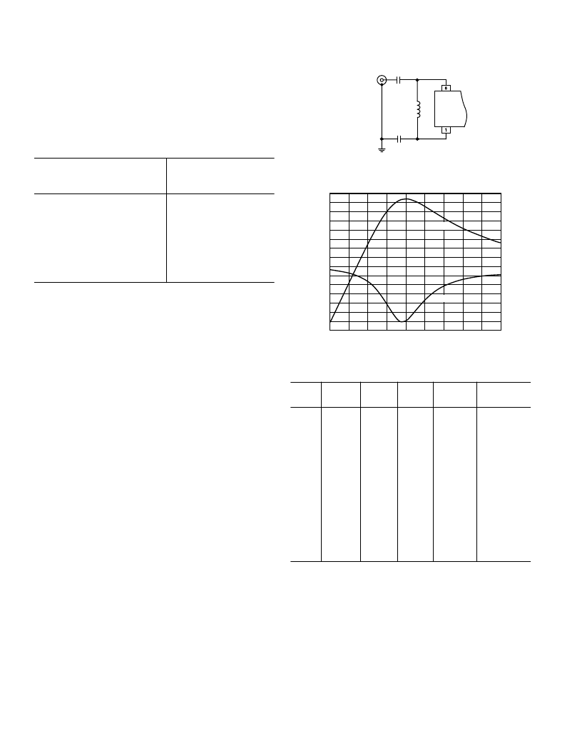
Narrow-Band Matching
Transformer coupling is useful in broadband applications. How-
ever, a magnetically-coupled transformer may not be convenient
in some situations. At high frequencies, it is often preferable to
use a narrow-band matching network, as shown in Figure 29.
This has several advantages. The same voltage gain is achieved,
providing increased sensitivity, but now a measure of selectively
is also introduced. The component count is low: two capacitors
and an inexpensive chip inductor. Further, by making these
capacitors unequal the amplitudes at INP and INM may be
equalized when driving from a single-sided source; that is, the
network also serves as a balun. Figure 30 shows the response for
a center frequency of 100MHz; note the very high attenuation
at low frequencies. The high-frequency attenuation is due to the
input capacitance of the log amp.
C1
C2
INHI
INLO
AD8310
SIGNAL
INPUT
L
M
Figure 29. Reactive Matching Network
FREQUENCY – MHz
14
13
12
11
10
4
3
2
1
0
–1
60
150
80
D
100
110
130
70
90
120
140
INPUT
GAIN
9
8
7
6
5
Figure 30. Response of 100 MHz Matching Network
Table II. Narrow-Band Matching Values
F
C
MHz
10
20
50
100
150
200
250
500
10
20
50
100
150
200
250
500
Z
IN
V
C1
pF
160
82
30
15
10
7.5
6.2
3.9
100
51
22
11
7.5
5.6
4.3
2.2
C2
pF
150
75
27
13
8.2
6.8
5.6
3.3
91
43
18
9.1
6.2
4.7
3.9
2.0
L
M
nH
3300
1600
680
270
220
150
100
39
5600
2700
1000
430
260
180
130
47
Voltage
Gain (dB)
13.3
13.4
13.4
13.4
13.2
12.8
12.3
10.9
10.4
10.4
10.6
10.5
10.3
10.3
9.9
6.8
45
44
46
50
57
57
50
54
103
102
99
98
101
95
92
114
相關(guān)PDF資料 |
PDF描述 |
|---|---|
| AD8315 | 50 dB GSM PA Controller |
| AD8315-EVAL | 50 dB GSM PA Controller |
| AD8315ACP-EVAL | 50 dB GSM PA Controller |
| AD8315ACP-REEL | 50 dB GSM PA Controller |
| AD8315ACP-REEL7 | 50 dB GSM PA Controller |
相關(guān)代理商/技術(shù)參數(shù) |
參數(shù)描述 |
|---|---|
| AD8310ARMZ | 功能描述:IC LOGARITHMIC AMP 95DB 8-MSOP RoHS:是 類別:集成電路 (IC) >> 線性 - 放大器 - 專用 系列:- 產(chǎn)品培訓(xùn)模塊:Lead (SnPb) Finish for COTS Obsolescence Mitigation Program 標(biāo)準(zhǔn)包裝:60 系列:- 類型:可變?cè)鲆娣糯笃?應(yīng)用:CATV 安裝類型:表面貼裝 封裝/外殼:20-WQFN 裸露焊盤 供應(yīng)商設(shè)備封裝:20-TQFN-EP(5x5) 包裝:托盤 |
| AD8310ARMZ | 制造商:Analog Devices 功能描述:Operational Amplifier (Op-Amp) IC |
| AD8310ARMZ-REEL1 | 制造商:AD 制造商全稱:Analog Devices 功能描述:Fast, Voltage-Out DC-440 MHz, 95 dB Logarithmic Amplifier |
| AD8310ARMZ-REEL7 | 功能描述:IC AMP LOGARITHMIC 8MSOP RoHS:是 類別:集成電路 (IC) >> 線性 - 放大器 - 專用 系列:- 產(chǎn)品培訓(xùn)模塊:Lead (SnPb) Finish for COTS Obsolescence Mitigation Program 標(biāo)準(zhǔn)包裝:60 系列:- 類型:可變?cè)鲆娣糯笃?應(yīng)用:CATV 安裝類型:表面貼裝 封裝/外殼:20-WQFN 裸露焊盤 供應(yīng)商設(shè)備封裝:20-TQFN-EP(5x5) 包裝:托盤 |
| AD8310ARMZ-REEL71 | 制造商:AD 制造商全稱:Analog Devices 功能描述:Fast, Voltage-Out DC-440 MHz, 95 dB Logarithmic Amplifier |
發(fā)布緊急采購(gòu),3分鐘左右您將得到回復(fù)。