- 您現(xiàn)在的位置:買賣IC網(wǎng) > PDF目錄375235 > AD7013ARS (ANALOG DEVICES INC) CMOS TIA IS-54 Baseband Receive Port PDF資料下載
參數(shù)資料
| 型號: | AD7013ARS |
| 廠商: | ANALOG DEVICES INC |
| 元件分類: | 通信及網(wǎng)絡(luò) |
| 英文描述: | CMOS TIA IS-54 Baseband Receive Port |
| 中文描述: | SPECIALTY TELECOM CIRCUIT, PDSO28 |
| 封裝: | SSOP-28 |
| 文件頁數(shù): | 16/20頁 |
| 文件大小: | 591K |
| 代理商: | AD7013ARS |
–16–
REV. A
AD7013
PCB Layout Considerations
The use of an analog ground plane is recommended, where the
ground plane extends around the analog circuitry. Both AGND and
DGND should be externally tied together and connected to the
analog ground plane.
Good power supply decoupling is very important for best ADC
performance. A 0.1
μ
F ceramic decoupling capacitor should be
connected between V
AA
and the ground plane. The physical place-
ment of the capacitor (surface mount if possible) is important and
should be placed as close to the pin of the device as is physically
possible. This is also applied to the V
DD
pin. Poor power supply
decoupling can lead to a degradation in ADC offsets and SNR.
The Bypass pin should be decoupled to the ground plane using a
10 nF capacitor. Large capacitor values are not recommended as
this can cause the reference not to reach its final value, on power
up, before ADC autocalibration has commenced.
Capacitive loading of digital outputs should be minimized as much
as possible if power dissipation is a critical factor. The charging
and discharging of external load capacitances can be a significant
contribution to power dissipation, especially when the AD7013 is in
a low power sleep mode as the DxCLK remains active.
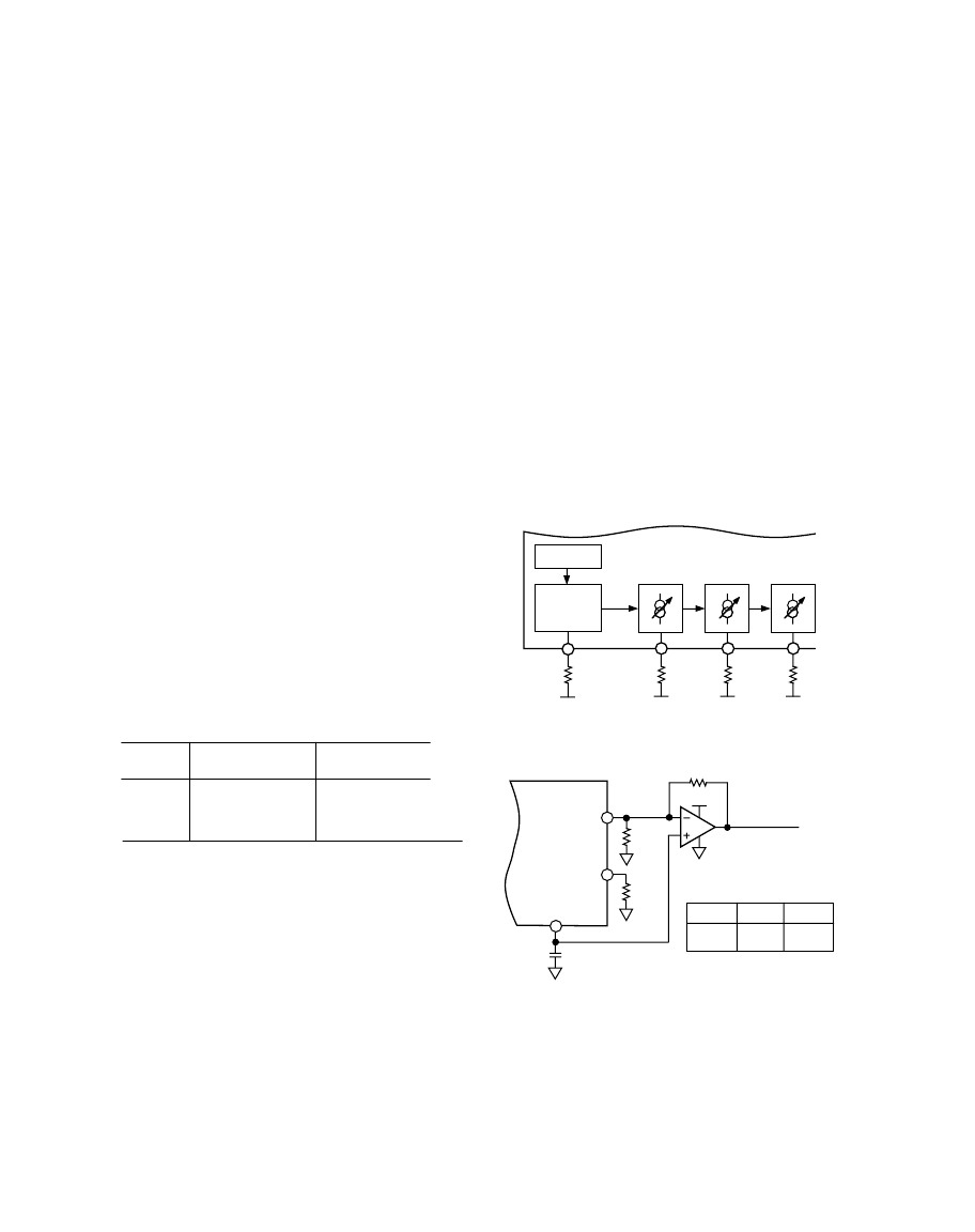
10-BIT
AUX DAC1
AGND
AGND
AGND
AGND
8-BIT
AUX DAC2
8-BIT
AUX DAC3
R
SET
FULL–SCALE
ADJUST
CONTROL
V
(1.23V)
AD7013
18k
4.5k
9k
9k
Figure 22. AUX DACs
AD7013
AUX DAC1,
AUX DAC2
OR AUX DAC3
FS ADJUST
10nF
BYPASS
≈
1 TO 4 VOLTS
+5V
OP-295
R
LOAD
R
FB
R
SET
18k
AUX DAC
R
LOAD
R
FB
10-BIT
8-BIT
2.4k
11k
5.4k
4.9k
Figure 23. External Op Amp Circuitry to Extend Output
Voltage Range
Low Sampling Rate (CR10 = 0)
The timing diagram for the receive interface is shown in Figure 4.
The output word rate per channel is equal to 48.6 kHz (MCLK/
128) which corresponds to two times the symbol rate. The low
sampling rate operates in a similar manner to that described for the
high sampling rate.
AUXILIARY DACs
One 10-bit auxiliary DAC and two 8-bit auxiliary DACs are
provided for extra control functions such as automatic gain control,
automatic frequency control and power control. Figure 22
illustrates a simplified block diagram of the auxiliary DACs. The
AUX DACs consist of high impedance current sources, designed to
operate at very low currents while maintaining their DC accuracy.
The DACs are designed using a current segmented architecture.
The bit currents corresponding to each digital input are either
routed to the analog output (bit = 1) or to AGND (bit = 0).
Each of the auxiliary DACs has independent low power sleep
modes. The command register has three control bits CR17, CR16
and CR15 which control AUX DAC1, AUX DAC2 and AUX
DAC3 respectively. A logic 0 represents low power sleep mode and
a logic 1 represents normal operation.
The full-scale currents of the auxiliary DACs are controlled by a
single external resistor, R
SET
, connected between the FS ADJUST
pin and AGND. The relationship between full-scale current and
R
SET
is given as follows:
10-
Bit AUX DAC
AUX DAC
FULL SCALE
(
mA
) = 7992
×
V
REF
(
V
)/
R
SET
(
)
8-
Bit AUX DACs
AUX DAC
FULL SCALE
(
mA
) = 3984
×
V
REF
(
V
)/
R
SET
(
)
By using smaller values of R
SET
, thereby increasing AUX DAC full-
scale current, improved INL and DNL performance is possible as
shown in Table V.
Digital Interface
Communication with the Command register, auxiliary DACs, ADC
offset registers and ADC vernier is accomplished via the 3-pin serial
interface. Either one of two loading formats may be used to write
to any of the AD7013’s internal registers. The first format consists
of a single 16-bit serial word to write to any internal register (Table
III). The second format consists of five 16-bit serial words, where
only the last 6 bits in each 16-bit word are used to load five 2-bit
data nibbles. The load sequence for this format is given is Table IV.
The second format is only enable when the Register Address 3 is
used as the destination register as shown in Table I.
Table V. AUX DAC1 INL and DNL as a Function of R
SET
18 k
9 k
4.5 k
–1.45
+1.22
+1.18
+1.83
+1.59
+1.38
Worst Case
INL (LSBs)
Worst Case
DNL (LSBs)
R
SET
相關(guān)PDF資料 |
PDF描述 |
|---|---|
| AD7013 | CMOS TIA IS-54 Baseband Receive Port(CMOS 基帶接收口) |
| AD7015 | Complete 3 V GSM/DCS1800 Codec(GSM/DCS1800 編碼譯碼器) |
| AD704AN | Quad Picoampere Input Current Bipolar Op Amp |
| AD704AQ | MB 55C 55#20 SKT RECP |
| AD704AR | MB 8C 8#12 PIN RECP |
相關(guān)代理商/技術(shù)參數(shù) |
參數(shù)描述 |
|---|---|
| AD7013ARS-REEL | 制造商:未知廠家 制造商全稱:未知廠家 功能描述:RF/Baseband Circuit |
| AD7015 | 制造商:AD 制造商全稱:Analog Devices 功能描述:GSM Baseband Processing Chipset |
| AD7015AST | 制造商:Rochester Electronics LLC 功能描述:- Bulk 制造商:Analog Devices 功能描述: |
| AD-7017 | 制造商:BOTHHAND 制造商全稱:Bothhand USA, LP. 功能描述:ADSL LINE TRANSFORMER |
| AD-702 | 制造商:Alarm Suppliers 功能描述: |
發(fā)布緊急采購,3分鐘左右您將得到回復(fù)。