- 您現(xiàn)在的位置:買賣IC網(wǎng) > PDF目錄375235 > AD7013 (Analog Devices, Inc.) CMOS TIA IS-54 Baseband Receive Port(CMOS 基帶接收口) PDF資料下載
參數(shù)資料
| 型號(hào): | AD7013 |
| 廠商: | Analog Devices, Inc. |
| 英文描述: | CMOS TIA IS-54 Baseband Receive Port(CMOS 基帶接收口) |
| 中文描述: | 電信行業(yè)協(xié)會(huì)的CMOS的IS - 54帶接收端口(的CMOS基帶接收口) |
| 文件頁數(shù): | 9/20頁 |
| 文件大小: | 599K |
| 代理商: | AD7013 |
REV. A
AD7013
–9–
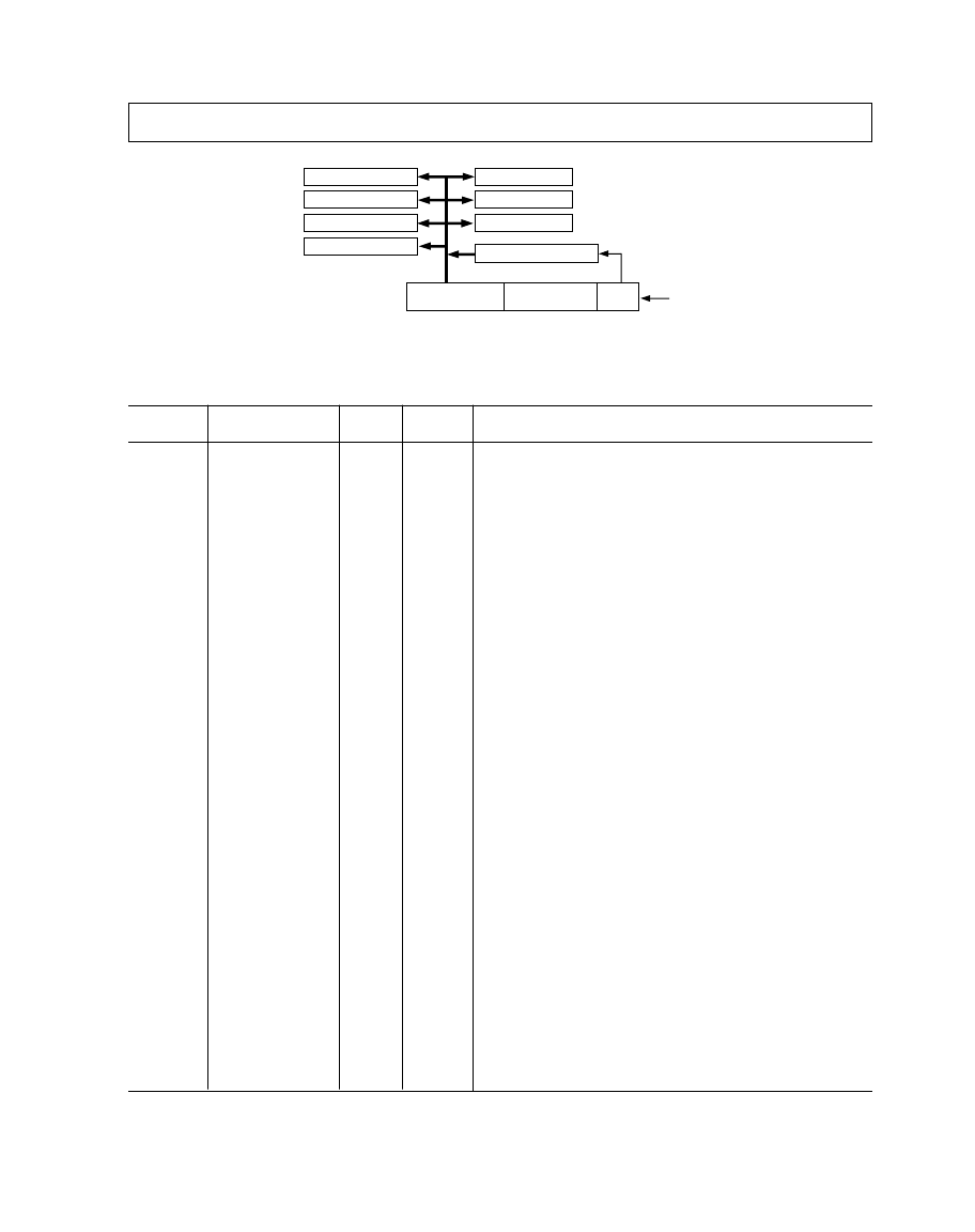
Register
Name
Address
A2
Register
Size
Reset
State
A3
A1
A0
Description
COMMAND
0
0
1
0
9 Bits
All Zeros
The COMMAND register is used to select various operating modes
of the AD7013. A detailed description of the COMMAND register
is given in Table II.
The VERNIER register allows additional group delay to be
introduced into the I and Q ADCs. This provides a means to vary
the ADC sampling instant.
The contents of the IRx OFFSET register are substracted from the
I channel ADC word. When autocalibration is selected, this register
is automatically loaded by the AD7013 at the beginning of
a normal operation. When user calibration is selected, this register
can be externally loaded with a twos complement offset 10-bit
word to be subtracted from subsequent ADC samples.
The contents of the QRx OFFSET register are substracted from
the Q channel ADC word. When auto calibration is selected, this
register is automatically loaded by the AD7013 at the beginning of
a normal operation. When user calibration is selected this register
can be externally loaded with a twos complement offset 10-bit
word to be subtracted from subsequent ADC samples.
The 10-bit auxiliary DAC current output is determined by this register.
The output current is equal to {AUX DAC1
FULL SCALE
* N/2
10
} where
N is the 10-bit word contained in the AUX DAC1 register and
AUX DAC1
FULL SCALE
is determined by the value of R
SET
connected
between FSADJUST and AGND.
The 8-bit auxiliary DAC current output is determined by this register.
The output current is equal to {AUX DAC1
FULL SCALE
* N/2
8
}
where N is the 8-bit word contained in the AUX DAC2 register
and AUX DAC2
FULL SCALE
is determined by the value of RSET
connected between FS ADJUST and AGND.
The 8-bit auxiliary DAC current output is determined by this register.
The output current is equal to {AUX DAC3
FULL SCALE
* N/2
8
}
where N is the 8-bit word contained in the AUX DAC3 register
and AUX DAC3
FULL SCALE
is determined by the value of R
SET
connected between FS ADJUST and AGND.
When this address in selected, all of the internal registers are initialized
to their reset state.
When this address is used, a special loading sequence, as shown in
Table IV, is used to write to any of the internal registers.
No Action.
No Action.
VERNIER
0
1
0
0
4 Bits
All Zeros
IRx OFFSET
0
1
0
1
10 Bits
All Zeros
QRx OFFSET
0
1
1
0
10 Bits
All Zeros
AUX DAC1
0
1
1
1
10 Bits
All Zeros
AUX DAC2
1
0
0
0
8 Bits
All Zeros
AUX DAC3
1
0
0
1
8 Bits
All Zeros
RESET
0
0
0
1
N/A
N/A
6-Bit LOAD
0
0
1
1
N/A
N/A
N/A
N/A
0
1
0
1
0
1
0
1
N/A
N/A
N/A
N/A
Table I. Description and Address Map for AD7013 Internal Registers
IRx OFFSET ADJUST
Rx SAMPLING VERNIER
AUX DAC1
AUX DAC2
QRx OFFSET ADJUST
AUX DAC3
DATA IN
A3 – A0
S1, S0
COMMAND REGISTER
6-BIT LOAD DATA BUFFER
DB9 – DB0
MSB
LSB
16-BIT SERIAL WORD
Figure 6. AD7013 Registers
相關(guān)PDF資料 |
PDF描述 |
|---|---|
| AD7015 | Complete 3 V GSM/DCS1800 Codec(GSM/DCS1800 編碼譯碼器) |
| AD704AN | Quad Picoampere Input Current Bipolar Op Amp |
| AD704AQ | MB 55C 55#20 SKT RECP |
| AD704AR | MB 8C 8#12 PIN RECP |
| AD704AR-REEL | Quad Picoampere Input Current Bipolar Op Amp |
相關(guān)代理商/技術(shù)參數(shù) |
參數(shù)描述 |
|---|---|
| AD7013ARS | 制造商:AD 制造商全稱:Analog Devices 功能描述:CMOS TIA IS-54 Baseband Receive Port |
| AD7013ARS-REEL | 制造商:未知廠家 制造商全稱:未知廠家 功能描述:RF/Baseband Circuit |
| AD7015 | 制造商:AD 制造商全稱:Analog Devices 功能描述:GSM Baseband Processing Chipset |
| AD7015AST | 制造商:Rochester Electronics LLC 功能描述:- Bulk 制造商:Analog Devices 功能描述: |
| AD-7017 | 制造商:BOTHHAND 制造商全稱:Bothhand USA, LP. 功能描述:ADSL LINE TRANSFORMER |
發(fā)布緊急采購,3分鐘左右您將得到回復(fù)。