- 您現(xiàn)在的位置:買賣IC網(wǎng) > PDF目錄375235 > AD7013 (Analog Devices, Inc.) CMOS TIA IS-54 Baseband Receive Port(CMOS 基帶接收口) PDF資料下載
參數(shù)資料
| 型號: | AD7013 |
| 廠商: | Analog Devices, Inc. |
| 英文描述: | CMOS TIA IS-54 Baseband Receive Port(CMOS 基帶接收口) |
| 中文描述: | 電信行業(yè)協(xié)會的CMOS的IS - 54帶接收端口(的CMOS基帶接收口) |
| 文件頁數(shù): | 12/20頁 |
| 文件大?。?/td> | 599K |
| 代理商: | AD7013 |
–12–
REV. A
AD7013
V
BIAS
IRx
V
V
BIAS
+ 0.65
V
BIAS
– 0.65
IRx
ADC CODE
10 … 00
00 … 00
01 … 11
Figure 11. ADC Transfer Function for Differential
Operation
V
BIAS
IRx
V
V
BIAS
+ 1.3
V
BIAS
– 1.3
IRx
ADC CODE
10 … 00
00 … 00
01 … 11
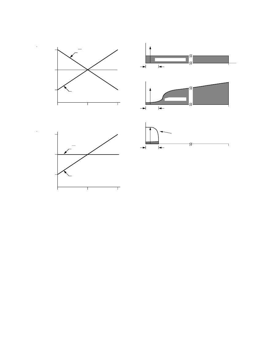
SIGMA-DELTA ADC
The AD7013 receive channels employ a sigma-delta conversion
technique, which provides a high resolution 15-bit output for both I
and Q channels with system filtering being implemented on-chip.
The output of the switched-capacitor filter is continuously sampled
at MCLK/8, by a charge-balanced modulator, and is converted
into a digital pulse train whose duty cycle contains the digital
information. Due to the high oversampling rate which spreads the
quantization noise from 0 to f
S
/2, the noise energy which is
contained in the band of interest is reduced (Figure 13a). To
reduce the quantization noise still further, a high order modulator is
employed to shape the noise spectrum, so that most of the noise
energy is shifted out of the band of interest (Figure 13b).
The digital filter that follows the modulator removes the large out
of band quantization noise (Figure 13c), while converting the
digital pulse train into parallel 15-bit wide binary data. The 15-bit
I and Q data plus an I/Q flag bit is made available, via a serial
interface, as a 16-bit word, MSB first.
Figure 12. ADC Transfer Function for Single-Ended
Operation
Digital Filter
important functions. First, they remove the out of band quantiza-
tion noise which is shaped by the analog modulator. Second, they
are also designed to perform system level filtering, providing the
Root-Raised Cosine filter as required for TIA IS-54.
Since digital filtering occurs after the A/D conversion process, it can
remove noise injected during the conversion process. Analog
filtering cannot do this. Also, the digital filter combines low
passband ripple with a steep roll off, while also maintaining a linear
phase response. This is very difficult to achieve with analog filters.
Filter Characteristics
The digital filter is a 256-tap FIR filter, clocked at 1/8 the master
clock frequency. A choice of two frequency responses are available:
a Root-Raised Cosine response (CR11 = 0) and a brick wall
response at 11.4 kHz (CR11 = 1) for analog mode. Figure 16 and
Figure 17 illustrate the respective frequency responses for both
digital mode and analog mode while Figure 18 compares the low
frequency response of the digital filters.
Due to the low-pass nature of the receive filters there is a settling
time associated with step input functions. Output data will not be
meaningful until all the digital filter taps have been loaded with
data samples taken after the step change. Hence, the AD7013
digital filters have a settling time of 256
×
8t
1
(i.e., 329.2
μ
s when
MCLK = 6.2208 MHz and 400
μ
s when MCLK = 5.12 MHz).
f
s/2
388.8kHz
QUANTIZATION NOISE
f
s/2
388.8kHzMHz
BAND OF
INTEREST
NOISE SHAPING
BAND OF
INTEREST
f
s/2
388.8kHz
BAND OF
INTEREST
ROOT RAISED COSINE FIR FILTER
a
b
b.
c
Figure 13. a. Effect of High Oversampling Ratio.
b. Use of Noise Shaping to Further Improve SNR.
c. Use of Digital Filtering to Remove the Out of Band
Quantization Noise
a.
c.
相關(guān)PDF資料 |
PDF描述 |
|---|---|
| AD7015 | Complete 3 V GSM/DCS1800 Codec(GSM/DCS1800 編碼譯碼器) |
| AD704AN | Quad Picoampere Input Current Bipolar Op Amp |
| AD704AQ | MB 55C 55#20 SKT RECP |
| AD704AR | MB 8C 8#12 PIN RECP |
| AD704AR-REEL | Quad Picoampere Input Current Bipolar Op Amp |
相關(guān)代理商/技術(shù)參數(shù) |
參數(shù)描述 |
|---|---|
| AD7013ARS | 制造商:AD 制造商全稱:Analog Devices 功能描述:CMOS TIA IS-54 Baseband Receive Port |
| AD7013ARS-REEL | 制造商:未知廠家 制造商全稱:未知廠家 功能描述:RF/Baseband Circuit |
| AD7015 | 制造商:AD 制造商全稱:Analog Devices 功能描述:GSM Baseband Processing Chipset |
| AD7015AST | 制造商:Rochester Electronics LLC 功能描述:- Bulk 制造商:Analog Devices 功能描述: |
| AD-7017 | 制造商:BOTHHAND 制造商全稱:Bothhand USA, LP. 功能描述:ADSL LINE TRANSFORMER |
發(fā)布緊急采購,3分鐘左右您將得到回復(fù)。