- 您現(xiàn)在的位置:買賣IC網(wǎng) > PDF目錄375235 > AD7010ARS (ANALOG DEVICES INC) MIL-spec connector accessory PDF資料下載
參數(shù)資料
| 型號: | AD7010ARS |
| 廠商: | ANALOG DEVICES INC |
| 元件分類: | 通信及網(wǎng)絡(luò) |
| 英文描述: | MIL-spec connector accessory |
| 中文描述: | SPECIALTY TELECOM CIRCUIT, PDSO24 |
| 封裝: | SSOP-24 |
| 文件頁數(shù): | 8/8頁 |
| 文件大小: | 249K |
| 代理商: | AD7010ARS |
AD7010
REV. B
–8–
C
P
I Channel – Volts
1.2
–1.2
1.2
0
–0.8
–0.8
–0.4
–1.2
0.8
0.4
0.8
0.4
0
–0.4
Q
Figure 13. AD7010 I vs. Q Waveforms when Transmitting
Random Data
I Channel – Volts
Q
1.2
–1.2
1.2
0
–0.8
–0.8
–0.4
–1.2
0.8
0.4
0.8
0.4
0
–0.4
Figure 14. AD7010 I vs. Q Waveforms Filtered by an Ideal
Root Raised Cosine Receive Filter
When BIN goes high, the READY signal goes low on the next
rising edge of MCLK and T xCLK becomes active after a further
two MCLK cycles. T xCLK can be used to clock out the trans-
mit data from the ASIC or DSP on the rising edge of T xCLK
and the AD7010 will latch T xDAT A on the falling edge of
T xCLK .
When BIN is brought low, the AD7010 will continue to clock in
the current Di-bit symbol (X
N+4
, Y
N+4
) and will continue for a
further eight T xCLK cycles (four symbols). After the final
T xCLK , READY goes high waiting for BIN to be brought high
to begin the next transmit burst.
When Power is brought low, this puts the transmit section into a
low power sleep mode, drawing minimal current. T he analog
outputs go high impedance while in low power sleep mode.
MODE1 = DGND; MODE2 = V
DD
: Frequency Test Mode
A special FT EST (Frequency T EST ) mode is provided for the
customer, where no phase modulation takes place and the
modulator outputs remain static. IT x is set to zero and QT x is
set to full scale as Figure 2 illustrates. However, the normal
ramp-up/down envelope is still applied during the beginning and
end of a burst.
MODE
1 =
V
DD
;
MODE
2 =
DGND
:
Factory Test Mode
MODE
1 =
MODE
2 = V
DD
:
Factory Test Mode
T hese modes are reserved for factory test only and should not be
used by the customer for correct device operation.
I Channel – Volts
Q
1.2
–1.2
1.2
0
–0.8
–0.8
–0.4
–1.2
0.8
0.4
0.8
0.4
0
–0.4
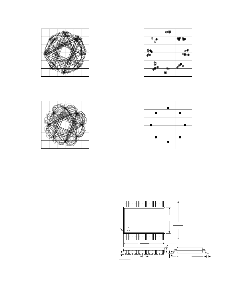
Figure 15. AD7010 Transmit Constellation Diagram
I Channel – Volts
Q
1.2
–1.2
1.2
0
–0.8
–0.8
–0.4
–1.2
0.8
0.4
0.8
0.4
0
–0.4
Figure 16. AD7010 Constellation Diagram when Filtered
by an Ideal Root Raised Cosine Receive Filter
OUT LINE DIME NSIONS
Dimensions are shown in inches and (mm).
24-Lead SSOP (RS-24)
1. LEAD NO. 1 IDENTIFIED BY A DOT.
2. LEADS WILL BE EITHER TIN PLATED OR SOLDER DIPPED
IN ACCORDANCE WITH MIL-M-38510 REQUIREMENTS
0.009 (0.229)
0.005 (0.127)
0.037 (0.94)
0.022 (0.559)
8
°
0
°
0.0256 (0.65)
BSC
0.07 (1.78)
0.066 (1.67)
0.328 (8.33)
0.318 (8.08)
0.008 (0.203)
0.002 (0.050)
PIN 1
0.311 (7.9)
0.301 (7.64)
0.212 (5.38)
0.205 (5.207)
1
24
13
12
相關(guān)PDF資料 |
PDF描述 |
|---|---|
| AD7010 | CMOS JDC DQPSK Baseband Transmit Port(CMOS 基帶傳輸口) |
| AD7011 | CMOS, ADC p/4 DQPSK Baseband Transmit Port |
| AD7011ARS | MB 4C 4#12 PIN RECP |
| AD7013ARS | CMOS TIA IS-54 Baseband Receive Port |
| AD7013 | CMOS TIA IS-54 Baseband Receive Port(CMOS 基帶接收口) |
相關(guān)代理商/技術(shù)參數(shù) |
參數(shù)描述 |
|---|---|
| AD7011 | 制造商:AD 制造商全稱:Analog Devices 功能描述:CMOS, ADC p/4 DQPSK Baseband Transmit Port |
| AD7011ARS | 制造商:Analog Devices 功能描述:Quadrature Mod 24-Pin SSOP |
| AD7011ARS-REEL | 制造商:Analog Devices 功能描述:Quadrature Mod 24-Pin SSOP T/R 制造商:Rochester Electronics LLC 功能描述:- Tape and Reel |
| AD7013 | 制造商:AD 制造商全稱:Analog Devices 功能描述:CMOS TIA IS-54 Baseband Receive Port |
| AD7013ARS | 制造商:AD 制造商全稱:Analog Devices 功能描述:CMOS TIA IS-54 Baseband Receive Port |
發(fā)布緊急采購,3分鐘左右您將得到回復(fù)。