- 您現(xiàn)在的位置:買賣IC網(wǎng) > PDF目錄11674 > AD598JRZ (Analog Devices Inc)IC LVDT SGNL COND OSC/REF 20SOIC PDF資料下載
參數(shù)資料
| 型號: | AD598JRZ |
| 廠商: | Analog Devices Inc |
| 文件頁數(shù): | 10/16頁 |
| 文件大?。?/td> | 0K |
| 描述: | IC LVDT SGNL COND OSC/REF 20SOIC |
| 標準包裝: | 1 |
| 類型: | 信號調節(jié)器 |
| 輸入類型: | 電壓 |
| 輸出類型: | 電壓 |
| 接口: | LVDT |
| 電流 - 電源: | 15mA |
| 安裝類型: | 表面貼裝 |
| 封裝/外殼: | 20-SOIC(0.295",7.50mm 寬) |
| 供應商設備封裝: | 20-SOIC W |
| 包裝: | 管件 |
| 產(chǎn)品目錄頁面: | 791 (CN2011-ZH PDF) |
NOTES
1V
A and VB represent the Mean Average Deviation (MAD) of the detected sine waves. Note that for this Transfer Function to linearly represent positive displacement,
the sum of VA and VB of the LVDT must remain constant with stroke length. See “Theory of Operation.” Also see Figures 7 and 12 for R2.
2From T
MIN, to TMAX, the overall error due to the AD598 alone is determined by combining gain error, gain drift and offset drift. For example the worst case overall
error for the AD598AD from TMIN to TMAX is calculated as follows: overall error = gain error at +25°C (± 1% full scale) + gain drift from –40°C to +25°C (50 ppm/°C
of FS
× +65°C) + offset drift from –40°C to +25°C (50 ppm/°C of FS × +65°C) = ±1.65% of full scale. Note that 1000 ppm of full scale equals 0.1% of full scale.
Full scale is defined as the voltage difference between the maximum positive and maximum negative output.
3Nonlinearity of the AD598 only, in units of ppm of full scale. Nonlinearity is defined as the maximum measured deviation of the AD598 output voltage from a
straight line. The straight line is determined by connecting the maximum produced full-scale negative voltage with the maximum produced full-scale positive voltage.
4See Transfer Function.
5This offset refers to the (V
A–VB)/(VA+VB) input spanning a full-scale range of ± 1. [For (VA–VB)/(VA+VB) to equal +1, VB must equal zero volts; and correspondingly
for (VA–VB)/(VA+VB) to equal –1, VA must equal zero volts. Note that offset errors do not allow accurate use of zero magnitude inputs, practical inputs are limited to
100 mV rms.] The
± 1 span is a convenient reference point to define offset referred to input. For example, with this input span a value of R2 = 20 k would give
VOUT span a value of ± 10 volts. Caution, most LVDTs will typically exercise less of the ((V A–VB))/((VA+VB)) input span and thus require a larger value of R2 to
produce the
±10 V output span. In this case the offset is correspondingly magnified when referred to the output voltage. For example, a Schaevitz E100 LVDT
requires 80.2 k
for R2 to produce a ±10.69 V output and (V
A–VB)/(VA+VB) equals 0.27. This ratio may be determined from the graph shown in Figure 18,
(VA–VB)/(VA+VB) = (1.71 V rms – 0.99 V rms)/(1.71 V rms + 0.99 V rms). The maximum offset value referred to the ± 10.69 V output may be determined by
multiplying the maximum value shown in the data sheet (
±1% of FS by 1/0.27 which equals ±3.7% maximum. Similarly, to determine the maximum values of offset
drift, offset CMRR and offset PSRR when referred to the
± 10.69 V output, these data sheet values should also be multiplied by (1/0.27). For this example for the
AD598AD the maximum values of offset drift, PSRR offset and CMRR offset would be: 185 ppm/
°C of FS; 741 ppm/V and 741 ppm/V respectively when referred
to the
± 10.69 V output.
6For example, if the excitation to the primary changes by 1 dB, the gain of the system will change by typically 100 ppm.
7Output ripple is a function of the AD598 bandwidth determined by C2, C3 and C4. See Figures 16 and 17.
8R1 is shown in Figures 7 and 12.
9Excitation voltage drift is not an important specification because of the ratiometric operation of the AD598.
Specifications subject to change without notice.
Specifications shown in boldface are tested on all production units at final electrical test. Results from those tested are used to calculate outgoing quality levels. All
min and max specifications are guaranteed, although only those shown in boldface are tested on all production units.
AD598
THERMAL CHARACTERISTICS
θ
JC
θ
JA
SOIC Package
22
°C/W
80
°C/W
Side Brazed Package
25
°C/W
85
°C/W
ABSOLUTE MAXIMUM RATINGS
Total Supply Voltage +VS to –VS
. . . . . . . . . . . . . . . . . +36 V
Storage Temperature Range
R Package . . . . . . . . . . . . . . . . . . . . . . . . . –65
°C to +150°C
D Package . . . . . . . . . . . . . . . . . . . . . . . . . –65
°C to +150°C
Operating Temperature Range
AD598JR . . . . . . . . . . . . . . . . . . . . . . . . . . . . 0
°C to +70°C
AD598AD . . . . . . . . . . . . . . . . . . . . . . . . . . –40
°C to +85°C
Lead Temperature Range (Soldering 60 sec) . . . . . . . . +300
°C
Power Dissipation Up to +65
°C . . . . . . . . . . . . . . . . . . .1.2 W
Derates Above +65
°C . . . . . . . . . . . . . . . . . . . . . . . 12 mW/°C
ORDERING GUIDE
Temperature
Package
Model
Range
Description
Option
AD598JR
0
°C to +70°C
SOIC
R-20
AD598AD
–40
°C to +85C
Ceramic DIP
D-20
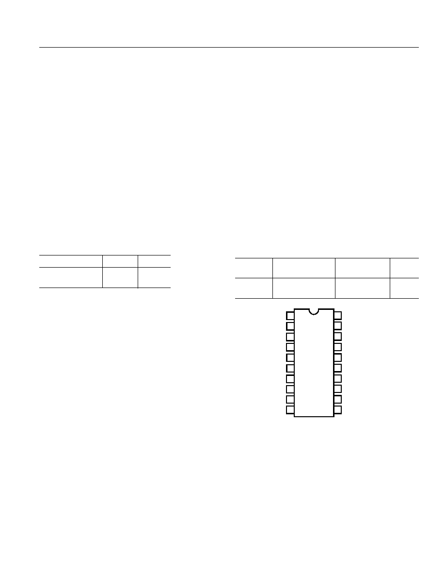
OFFSET 1
OFFSET 2
SIGNAL REFERENCE
SIGNAL OUTPUT
FEEDBACK
OUTPUT FILTER
A1 FILTER
A2 FILTER
EXC 1
EXC 2
LEVEL 1
LEVEL 2
FREQ 1
FREQ 2
B1 FILTER
B2 FILTER
1
2
3
4
5
6
7
8
9
10
11
12
13
14
16
15
17
18
19
20
–V
S
+V
S
AD598
TOP VIEW
(Not to Scale)
VB
VA
REV. A
–3–
相關PDF資料 |
PDF描述 |
|---|---|
| 221185-2 | CONN PLUG BNC 75 OHM DUAL CRIMP |
| AD698APZ | IC LVDT SIGNAL COND 28-PLCC |
| 221185-8 | CONN PLUG BNC 75 OHM DUAL CRIMP |
| AD693AD | IC SGNL COND 4-20MA TX 20-CDIP |
| AD9824KCPZ | IC CCD SIGNAL PROC 14BIT 48LFCSP |
相關代理商/技術參數(shù) |
參數(shù)描述 |
|---|---|
| AD598JRZ | 制造商:Analog Devices 功能描述:Signal Conditioner IC |
| AD598SD/883B | 制造商:Analog Devices 功能描述:LVDT Signal Conditioner 20-Pin SBCDIP 制造商:Analog Devices 功能描述:LVDT IC - Rail/Tube 制造商:Analog Devices 功能描述:MIL LVDT SIG COND 20-CDIP 制造商:Analog Devices 功能描述:IC SIGNAL CONDITIONER 制造商:Analog Devices Inc. 功能描述:Interface - Specialized IC LVDT Signal Conditioner |
| AD598SD/883B-MOOG | 制造商:Analog Devices 功能描述: |
| AD5T | 制造商:Opto 22 功能描述:I/O Module; 5 VDC @ 170 mA; 0 to degC; UL, CSA, CE Certified 制造商:Opto 22 功能描述:I/O MODULE 制造商:Opto 22 功能描述:I/O MODULE; Leaded Process Compatible:No; Peak Reflow Compatible (260 C):No; No. of Analog Inputs:1; No. of Digital Outputs:1; No. of Outputs:1; Resolution:12 Bits; Signal Input Type:J Thermocouple ;RoHS Compliant: No 制造商:Opto 22 功能描述:Access Module Analog J Thermocouple Input Isolated Ad5T |
| AD6 | 功能描述:保險絲 6A 415V AC / 250V DC RoHS:否 制造商:Littelfuse 產(chǎn)品:Surface Mount Fuses 電流額定值:0.5 A 電壓額定值:600 V 保險絲類型:Fast Acting 保險絲大小/組:Nano 尺寸:12.1 mm L x 4.5 mm W 安裝風格: 端接類型:SMD/SMT 系列:485 |
發(fā)布緊急采購,3分鐘左右您將得到回復。