- 您現(xiàn)在的位置:買賣IC網(wǎng) > PDF目錄360656 > 9Q512K32 (Aeroflex Inc.) UT9Q512K32 16Megabit SRAM MCM PDF資料下載
參數(shù)資料
| 型號(hào): | 9Q512K32 |
| 廠商: | Aeroflex Inc. |
| 英文描述: | UT9Q512K32 16Megabit SRAM MCM |
| 中文描述: | UT9Q512K32 16Megabit的SRAM億立方米 |
| 文件頁(yè)數(shù): | 2/14頁(yè) |
| 文件大小: | 135K |
| 代理商: | 9Q512K32 |
第1頁(yè)當(dāng)前第2頁(yè)第3頁(yè)第4頁(yè)第5頁(yè)第6頁(yè)第7頁(yè)第8頁(yè)第9頁(yè)第10頁(yè)第11頁(yè)第12頁(yè)第13頁(yè)第14頁(yè)
2
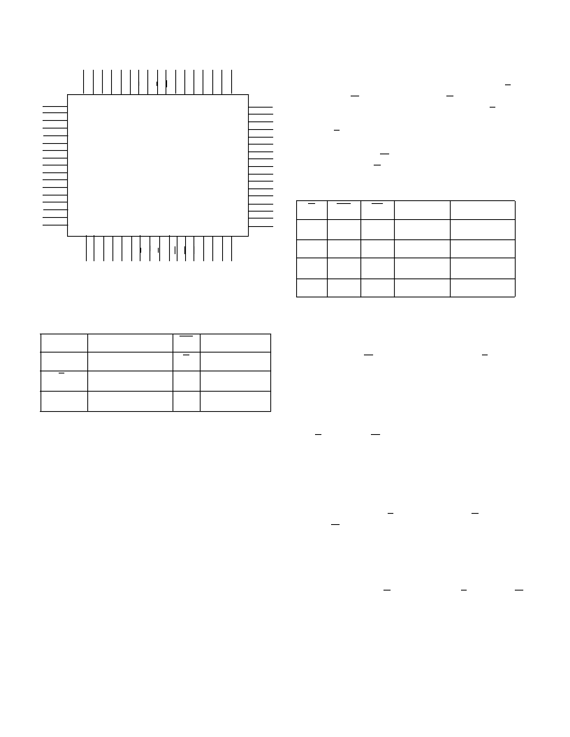
PIN NAMES
DEVICE OPERATION
The UT9Q512 has three control inputs called Enable 1 (En),
Write Enable (Wn), and Output Enable (G); 19 address inputs,
A(18:0); and eight bidirectional data lines, DQ(7:0). En Device
Enable controls device selection, active, and standby modes.
Asserting En enables the device, causes I
DD
to rise to its active
value, and decodes the 19 address inputs to select one of 524,288
words in the memory. Wn controls read and write operations.
During a read cycle, G must be asserted to enable the outputs.
Table 1. Device Operation Truth Table
Notes:
1. “X” is defined as a “don’t care” condition.
2. Device active; outputs disabled.
READ CYCLE
A combination of Wn greater than V
IH
(min) and En less than
V
IL
(max) defines a read cycle. Read access time is measured
from the latter of Device Enable, Output Enable, or valid address
to valid data output.
SRAM Read Cycle 1, the Address Access in figure 3a, is
initiated by a change in address inputs while the chip is enabled
with G asserted and Wn deasserted. Valid data appears on data
outputs DQ(7:0) after the specified t
AVQV
is satisfied. Outputs
remain active throughout the entire cycle. As long as Device
Enable and Output Enable are active, the address inputs may
change at a rate equal to the minimum read cycle time (t
AVAV
).
SRAM read Cycle 2, the Chip Enable - Controlled Access in
figure 3b, is initiated by En going active while G remains
asserted, Wn remains deasserted, and the addresses remain
stable for the entire cycle. After the specified t
ETQV
is satisfied,
the eight-bit word addressed by A(18:0) is accessed and appears
at the data outputs DQ(7:0).
SRAM read Cycle 3, the Output Enable - Controlled Access in
figure 3c, is initiated by G going active while En is asserted, Wn
is deasserted, and the addresses are stable. Read access time is
t
GLQV
unless t
AVQV
or t
ETQV
have not been satisfied.
A(18:0)
Address
Wn
Write Enable
DQn(7:0)
Data Input/Output
G
Output Enable
En
Enable
V
DD
Power
V
SS
Ground
10
11
12
13
14
15
16
17
18
19
20
21
22
23
24
25
26
60
59
58
57
56
55
54
53
52
51
50
49
48
47
46
45
44
9 8 7 6 5 4 3 2 1 68 67 66 65 64 63 62 61
27 28 29 30 31 32 33 34 35 36 37 38 39 40 41 42 43
Top View
DQ0(0)
DQ1(0)
DQ2(0)
DQ3(0)
DQ4(0)
DQ5(0)
DQ6(0)
DQ7(0)
V
DQ0(1)
DQ1(1)
DQ2(1)
DQ3(1)
DQ4(1)
DQ5(1)
DQ6(1)
DQ7(1)
DQ0(2)
DQ1(2)
DQ2(2)
DQ3(2)
DQ4(2)
DQ5(2)
DQ6(2)
DQ7(2)
V
DQ0(3)
DQ1(3)
DQ2(3)
DQ3(3)
DQ4(3)
DQ5(3)
DQ6(3)
DQ7(3)
N
A
A
A
A
A
A
E
V
S
E
W
A
A
A
A
A
V
D
V
D
A
A
A
A
A
A
E
G
E
A
W
W
W
A
N
N
Figure 2. 25ns SRAM Pinout (68)
G
Wn
En
I/O Mode
Mode
X
1
X
1
3-state
Standby
X
0
0
Data in
Write
1
1
0
3-state
Read
2
0
1
0
Data out
Read
相關(guān)PDF資料 |
PDF描述 |
|---|---|
| 9S12B128DGV1 | 9S12B128 Device Guide |
| 9S12C128DGV1 | MC9S12C Family Device User Guide |
| 9S12D32DGV1 | 9S12DGDJ64DGV1 Device Guide. also covers 9S12D64. 9S12A64. 9S12D32. and 9S12A32 devices |
| 9S12DJ64DGV1 | 9S12DJ64DG Device Guide. also covers 9S12D64. 9S12A64. 9S12D32 and 9S12A32 devices |
| 9S12DJ64-ZIP_PART2 | MC9S12DJ64 Users Guides. zip format. part 2 |
相關(guān)代理商/技術(shù)參數(shù) |
參數(shù)描述 |
|---|---|
| 9QA0-111-11-3.50 | 制造商:3M Electronic Products Division 功能描述:CABLE ASSY - Bulk |
| 9QA0-111-12-0.50 | 制造商:3M Electronic Products Division 功能描述:CABLE TWIN AXIAL 30AWG .5M 制造商:3M Electronic Products Division 功能描述:80001390170 |
| 9QA0-111-12-1.00 | 制造商:3M Electronic Products Division 功能描述:CABLE TWIN AXIAL 30AWG 1M 制造商:3M Electronic Products Division 功能描述:80001390188 |
| 9QA0-111-12-2.00 | 制造商:3M Electronic Products Division 功能描述:CABLE TWIN AXIAL 30AWG 2M 制造商:3M Electronic Products Division 功能描述:80001390196 |
| 9QA0-111-12-3.00 | 制造商:3M Electronic Products Division 功能描述:CABLE TWIN AXIAL 30AWG 3M 制造商:3M Electronic Products Division 功能描述:80001390204 |
發(fā)布緊急采購(gòu),3分鐘左右您將得到回復(fù)。