- 您現(xiàn)在的位置:買賣IC網(wǎng) > PDF目錄25570 > 9LPRS525AFLFT (INTEGRATED DEVICE TECHNOLOGY INC) SPECIALTY MICROPROCESSOR CIRCUIT, PDSO56 PDF資料下載
參數(shù)資料
| 型號: | 9LPRS525AFLFT |
| 廠商: | INTEGRATED DEVICE TECHNOLOGY INC |
| 元件分類: | 微控制器/微處理器 |
| 英文描述: | SPECIALTY MICROPROCESSOR CIRCUIT, PDSO56 |
| 封裝: | 0.300 INCH, ROHS COMPLIANT, MO-118, SSOP-56 |
| 文件頁數(shù): | 12/21頁 |
| 文件大小: | 200K |
| 代理商: | 9LPRS525AFLFT |
IDTTM
PC MAIN CLOCK
1484D—01/31/11
ICS9LPRS525
PC MAIN CLOCK
2
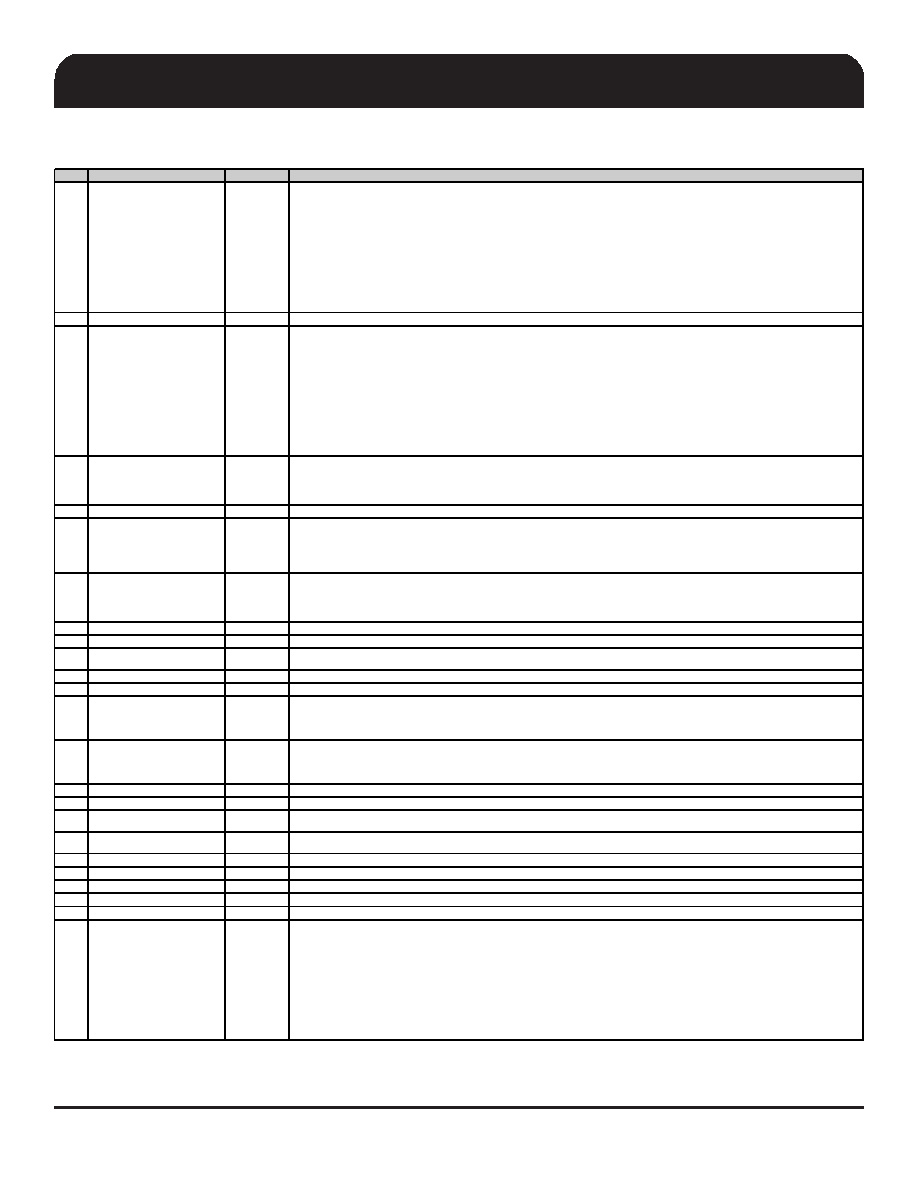
Pin Description
PIN #
PIN NAME
TYPE
DESCRIPTION
1
PCI0/CR#_A
I/O
3.3V PCI clock output or Clock Request control A for either SRC0 or SRC2 pair
The power-up default is PCI0 output, but this pin may also be used as a Clock Request control of SRC pair 0 or SRC pair 2 via SMBus. Before
configuring this pin as a Clock Request Pin, the PCI output must first be disabled in byte 2, bit 0 of SMBus address space . After the PCI output is
disabled (high-Z), the pin can then be set to serve as a Clock Request pin for either SRC pair 2 or pair 0 using the CRA#_EN bit located in byte 5 of
SMBUs address space.
Byte 5, bit 7
0 = PCI0 enabled (default)
1= CRA# enabled. Byte 5, bit 6 controls whether CRA# controls SRC0 or SRC2 pair
Byte 5, bit 6
0 = CRA# controls SRC0 pair (default),
1= CRA# controls SRC2 pair
2
VDDPCI
PWR
Power supply for PCI clocks, nominal 3.3V
3
PCI1/CR#_B
I/O
3.3V PCI clock output/Clock Request control B for either SRC1 or SRC4 pair
The power-up default is PCI1 output, but this pin may also be used as a Clock Request control of SRC pair 1 or SRC pair 4 via SMBus. Before
configuring this pin as a Clock Request Pin, the PCI output must first be disabled in byte 2, bit 1 of SMBus address space . After the PCI output is
disabled (high-Z), the pin can then be set to serve as a Clock Request pin for either SRC pair 1 or pair 4 using the CRB#_EN bit located in byte 5 of
SMBUs address space.
Byte 5, bit 5
0 = PCI1 enabled (default)
1= CRB# enabled. Byte 5, bit 6 controls whether CRB# controls SRC1 or SRC4 pair
Byte 5, bit 4
0 = CRB# controls SRC1 pair (default)
1= CRB# controls SRC4 pair
4PCI2/TME
I/O
3.3V PCI clock output / Trusted Mode Enable(TME) Latched Input. This pin is sampled on power-up as follows
0=Overclocking of CPU and SRC allowed
1=Overclocking of CPU and SRC NOT allowed
After being sampled on power-up, this pin becomes a 3.3V PCI Output
5
PCI3/CFG0
I/O
3.3V PCI clock output/Configuration Strap. See PCI3 Configuration Table for more information
6
PCI4/SRC5_EN
I/O
3.3V PCI clock output / SRC5 pair or PCI_STOP#/CPU_STOP# enable strap. On powerup, the logic value on this pin determines if the SRC5 pair is
enabled or if CPU_STOP#/PCI_STOP# is enabled (pins 29 and 30). The latched value controls the pin function on pins 29 and 30 as follows
0 = PCI_STOP#/CPU_STOP#
1 = SRC5/SRC5#
7
PCI_F5/ITP_EN
I/O
Free running PCI clock output and ITP/SRC8 enable strap. This output is not affected by the state of the PCI_STOP# pin. On powerup, the state of
this pin determines whether pins 38 and 39 are an ITP or SRC pair.
0 =SRC8/SRC8#
1 = ITP/ITP#
8
GNDPCI
PWR
Ground pin for the PCI outputs
9
VDD48
PWR
Power pin for the 48MHz output and PLL.3.3V
10
USB_48MHz/FSLA
I/O
3.3V tolerant input for CPU frequency selection. Refer to input electrical characteristics for Vil_FS and Vih_FS values. / Fixed 48MHz USB clock
output. 3.3V.
11
GND48
PWR
Ground pin for the 48MHz outputs
12
VDD96IO
PWR
Power supply for DOT96 outputs, 1.05V to 3.3V.
13
DOTT_96_LRS/SRCT0_LRS
OUT
True clock of low power differential SRC or DOT96 with integrated 33 ohm Rs. The power-up default function is SRC0. After powerup, this pin function
may be changed to DOT96 via SMBus Byte 1, bit 7 as follows:
0= SRC0
1=DOT96
14
DOTC_96_LRS/SRCC0_LRS
OUT
Complement clock of low power differential SRC or DOT96 with integrated 33 ohm Rs. The power-up default function is SRC0#. After powerup, this
pin function may be changed to DOT96# via SMBus Byte 1, bit 7 as follows
0= SRC0#
1=DOT96#
15
GND
PWR
Ground pin.
16
VDD
PWR
Power supply, nominal 3.3V
17
SRCT1_LRS/SE1
OUT
True clock of low power differential SRC1 clock pair with integrated 33 ohm Rs. / 3.3V single-ended output. The powerup default is 100 MHz SRC, -
0.5% downspread. The pin function may be changed via SMBus B1b[4:1]
18
SRCC1_LRS/SE2
OUT
Complement clock of low powerl differential SRC1 clock pair with integrated 33 ohm Rs / 3.3V single-ended output. The powerup default is 100 MHz
SRC, -0.5% downspread. The pin function may be changed via SMBus B1b[4:1]
19
GND
PWR
Ground pin.
20
VDDPLL3IO
PWR
Power supply for PLL3 outputs. 1.05V to 3.3V.
21
SRCT2_LRS/SATAT_LRS
OUT
True clock of low power differentiall SRC/SATA clock pair with integrated Rs.
22
SRCC2_LRS/SATAC_LRS
OUT
Complement clock of low power differential push-pull SRC/SATA clock pair with integrated 33 ohm Rs.
23
GNDSRC
PWR
Ground pin for the SRC outputs
24
SRCT3_LRS/CR#_C
I/O
True clock of low power differential SRC clock pair with integrated 33 ohm Rs./ Clock Request control C for either SRC0 or SRC2 pair. The power-up
default is SRCCLK3 output, but this pin may also be used as a Clock Request control of SRC pair 0 or SRC pair 2 via SMBus. Before configuring this
pin as a Clock Request Pin, the SRC output must first be disabled in byte 4, bit 7 of SMBus address space . After the SRC output is disabled, the pin
can then be set to serve as a Clock Request pin for either SRC pair 2 or pair 0 using the CRC#_EN bit located in byte 5 of SMBUs address space.
Byte 5, bit 3
0 = SRCCLK3 enabled (default)
1= CRC# enabled. Byte 5, bit 2 controls whether CRC# controls SRC0 or SRC2 pair
Byte 5, bit 2
0 = CRC# controls SRC0 pair (default),
1= CRC# controls SRC2 pair
相關(guān)PDF資料 |
PDF描述 |
|---|---|
| 9LPRS535BFLF | SPECIALTY MICROPROCESSOR CIRCUIT, PDSO48 |
| 9LPRS535CFLF | SPECIALTY MICROPROCESSOR CIRCUIT, PDSO48 |
| 9LPRS535CGLFT | SPECIALTY MICROPROCESSOR CIRCUIT, PDSO48 |
| 9LPRS545BGLF | SPECIALTY MICROPROCESSOR CIRCUIT, PDSO48 |
| 9LPRS545CGLF | SPECIALTY MICROPROCESSOR CIRCUIT, PDSO48 |
相關(guān)代理商/技術(shù)參數(shù) |
參數(shù)描述 |
|---|---|
| 9LPRS525AGILF | 功能描述:時鐘合成器/抖動清除器 56-PIN CK505 COMPATIBLE RoHS:否 制造商:Skyworks Solutions, Inc. 輸出端數(shù)量: 輸出電平: 最大輸出頻率: 輸入電平: 最大輸入頻率:6.1 GHz 電源電壓-最大:3.3 V 電源電壓-最小:2.7 V 封裝 / 箱體:TSSOP-28 封裝:Reel |
| 9LPRS525AGILFT | 功能描述:時鐘合成器/抖動清除器 56-PIN CK505 COMPATIBLE RoHS:否 制造商:Skyworks Solutions, Inc. 輸出端數(shù)量: 輸出電平: 最大輸出頻率: 輸入電平: 最大輸入頻率:6.1 GHz 電源電壓-最大:3.3 V 電源電壓-最小:2.7 V 封裝 / 箱體:TSSOP-28 封裝:Reel |
| 9LPRS525AGLF | 功能描述:時鐘合成器/抖動清除器 56-PIN CK505 COMPATIBLE RoHS:否 制造商:Skyworks Solutions, Inc. 輸出端數(shù)量: 輸出電平: 最大輸出頻率: 輸入電平: 最大輸入頻率:6.1 GHz 電源電壓-最大:3.3 V 電源電壓-最小:2.7 V 封裝 / 箱體:TSSOP-28 封裝:Reel |
| 9LPRS525AGLFT | 功能描述:時鐘合成器/抖動清除器 56-PIN CK505 COMPATIBLE RoHS:否 制造商:Skyworks Solutions, Inc. 輸出端數(shù)量: 輸出電平: 最大輸出頻率: 輸入電平: 最大輸入頻率:6.1 GHz 電源電壓-最大:3.3 V 電源電壓-最小:2.7 V 封裝 / 箱體:TSSOP-28 封裝:Reel |
| 9LPRS535 | 制造商:IDT 制造商全稱:Integrated Device Technology 功能描述:48-pin CK505 for Intel Systems |
發(fā)布緊急采購,3分鐘左右您將得到回復(fù)。