- 您現(xiàn)在的位置:買賣IC網(wǎng) > PDF目錄25515 > 952703BF (INTEGRATED DEVICE TECHNOLOGY INC) 217.9 MHz, PROC SPECIFIC CLOCK GENERATOR, PDSO48 PDF資料下載
參數(shù)資料
| 型號: | 952703BF |
| 廠商: | INTEGRATED DEVICE TECHNOLOGY INC |
| 元件分類: | 時鐘產(chǎn)生/分配 |
| 英文描述: | 217.9 MHz, PROC SPECIFIC CLOCK GENERATOR, PDSO48 |
| 封裝: | GREEN, MO-118, SSOP-48 |
| 文件頁數(shù): | 17/19頁 |
| 文件大小: | 264K |
| 代理商: | 952703BF |
7
Integrated
Circuit
Systems, Inc.
ICS952703
Preliminary Product Preview
0813B—05/17/05
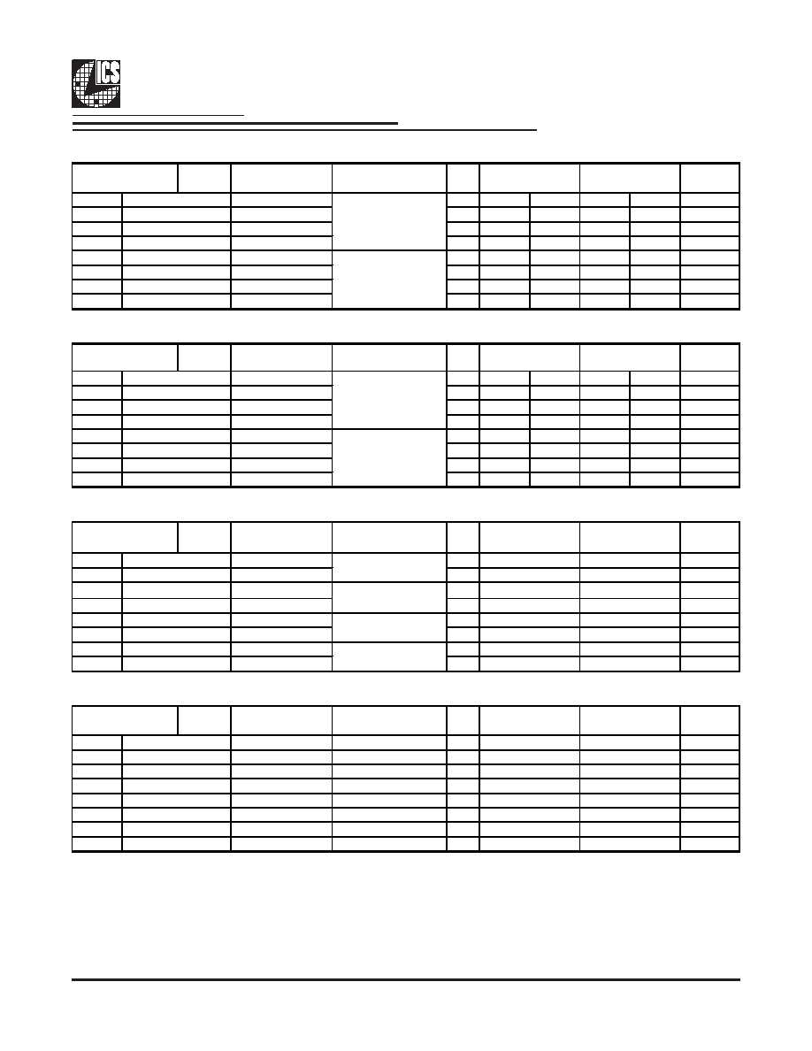
I
2C Table: Output Skew Control Register
Bit 7
PCISkw3
RW
0000:0
0100:150 1000:300 1100:450
X
Bit 6
PCISkw2
RW
0001:N/A 0101:N/A 1001:N/A 1101:600
X
Bit 5
PCISkw1
RW
0010:N/A 0110:N/A 1010:N/A 1110:750
X
Bit 4
PCISkw0
RW
0011:N/A 0111:N/A 1011:N/A 1111:900
X
Bit 3
AGPSkw3
RW
0000:0
0100:150 1000:300 1100:450
X
Bit 2
AGPSkw2
RW
0001:N/A 0101:N/A 1001:N/A 1101:600
X
Bit 1
AGPSkw1
RW
0010:N/A 0110:N/A 1010:N/A 1110:750
X
Bit 0
AGPSkw0
RW
0011:N/A 0111:N/A 1011:N/A 1111:900
X
I
2C Table: Output Divider Control Register
Bit 7
ZCLKDiv3
RW
0000:/2
0100:/4
1000:/8
1100:/16
X
Bit 6
ZCLKDiv2
RW
0001:/3
0101:/6
1001:/12
1101:/24
X
Bit 5
ZCLKDiv1
RW
0010:/5
0110:/10 1010:/20
1110:/40
X
Bit 4
ZCLKDiv0
RW
0011:/7
0111:/14 1011:/28
1111:/56
X
Bit 3
AGPDiv3
RW
0000:/2
0100:/4
1000:/8
1100:/16
X
Bit 2
AGPDiv2
RW
0001:/3
0101:/6
1001:/12
1101:/24
X
Bit 1
AGPDiv1
RW
0010:/5
0110:/10 1010:/20
1110:/40
X
Bit 0
AGPDiv0
RW
0011:/7
0111:/14 1011:/28
1111:/56
X
I
2C Table: Output Drive Control Register
Bit 7
PCIStr1
RW
1
Bit 6
PCIStr0
RW
1
Bit 5
PCIStr1
RW
1
Bit 4
PCIStr0
RW
1
Bit 3
PCIStr1
RW
1
Bit 2
PCIStr0
RW
1
Bit 1
AGPStr1
RW
1
Bit 0
AGPStr0
RW
1
I
2C Table: Reserved Register
Bit 7
Reserved
RW
1
Bit 6
Reserved
RW
1
Bit 5
Reserved
RW
1
Bit 4
Reserved
RW
1
Bit 3
Reserved
RW
1
Bit 2
Reserved
RW
1
Bit 1
Reserved
RW
1
Bit 0
Reserved
RW
1
CPU-AGP 7 Step Skew
Control (ps)
Type
-
Pin #
-
Byte 6
-
Name
Byte 5
Pin #
-
Byte 4
Pin #
Name
PCICLKF (1:0)
Strength Control
PCICLK (2:0) Strength
Control
PCICLK (5:3) Strength
Control
AGPCLK Strength
Control
Type
Name
Type
0
1
Type
PWD
-
Pin #
-
Byte 7
-
01
Control Function
AGP Divider Ratio
Programmaing Bits
-
ZCLK Divider Ratio
Programmaing Bits
1
01
0
00 = 0.63X
10 = 0.88X
01 = 0.75X
11 = 1.00X
00 = 0.63X
10 = 0.88X
--
10 = 0.90X
01 = 0.75X
11 = 1.00X
00 = 0.63X
10 = 0.88X
Control Function
CPU-PCI 7 Step Skew
Control (ps)
01 = 0.80X
11 = 1.00X
01 = 0.75X
11 = 1.00X
00 = 0.70X
相關PDF資料 |
PDF描述 |
|---|---|
| 952801CFLFT | 293.34 MHz, PROC SPECIFIC CLOCK GENERATOR, PDSO48 |
| 952807 | MODULAR TERMINAL BLOCK |
| 9528090000 | 10 A, MODULAR TERMINAL BLOCK, 1 DECK |
| 952830 | MODULAR TERMINAL BLOCK |
| 49830 | MODULAR TERMINAL BLOCK |
相關代理商/技術參數(shù) |
參數(shù)描述 |
|---|---|
| 952703BFLF | 制造商:Integrated Device Technology Inc 功能描述:952703BFLF - Rail/Tube |
| 952703BFLFT | 制造商:Integrated Device Technology Inc 功能描述:952703BFLFT - Tape and Reel |
| 952704 | 制造商:Weidmuller 功能描述:TB11, UL 1604, 2GP,SS -EA - Bulk |
| 952705 | 制造商:Weidmuller 功能描述:TB12, UL 1604, 2GP,SS -EA - Bulk |
| 952706 | 制造商:Weidmuller 功能描述:TB13, UL 1604, 2GP,SS -EA - Bulk |
發(fā)布緊急采購,3分鐘左右您將得到回復。