- 您現(xiàn)在的位置:買賣IC網(wǎng) > PDF目錄25515 > 952601EFLFT (INTEGRATED DEVICE TECHNOLOGY INC) 400 MHz, PROC SPECIFIC CLOCK GENERATOR, PDSO56 PDF資料下載
參數(shù)資料
| 型號(hào): | 952601EFLFT |
| 廠商: | INTEGRATED DEVICE TECHNOLOGY INC |
| 元件分類: | 時(shí)鐘產(chǎn)生/分配 |
| 英文描述: | 400 MHz, PROC SPECIFIC CLOCK GENERATOR, PDSO56 |
| 封裝: | 0.300 INCH, 0.025 INCH, GREEN, MO-118, SSOP-56 |
| 文件頁數(shù): | 21/27頁 |
| 文件大小: | 321K |
| 代理商: | 952601EFLFT |
第1頁第2頁第3頁第4頁第5頁第6頁第7頁第8頁第9頁第10頁第11頁第12頁第13頁第14頁第15頁第16頁第17頁第18頁第19頁第20頁當(dāng)前第21頁第22頁第23頁第24頁第25頁第26頁第27頁
3
Integrated
Circuit
Systems, Inc.
ICS952601
0701I—05/04/05
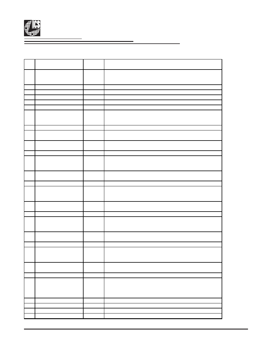
Pin Description (Continued)
PIN
#
PIN NAME
PIN TYPE
DESCRIPTION
29
3V66_4/VCH
OUT
66.66MHz clock output for AGP support. AGP-PCI should be
aligned with a skew window tolerance of 500ps.
VCH is 48MHz clock output for video controller hub.
30
SDATA
I/O
Data pin for SMBus circuitry, 5V tolerant.
31
48MHz_USB
OUT
48MHz clock output.
32
48MHz_DOT
OUT
48MHz clock output.
33
GND
PWR
Ground pin.
34
VDD48
PWR
Power pin for the 48MHz output.3.3V
35
Vtt_PWRGD#
IN
This 3.3V LVTTL input is a level sensitive strobe used to determine
when latch inputs are valid and are ready to be sampled. This is an
active low input.
36
VDD
PWR
Power supply for SRC clocks, nominal 3.3V
37
SRCCLKC
OUT
Complement clock of differential pair for S-ATA support.
+/- 300ppm accuracy required.
38
SRCCLKT
OUT
True clock of differential pair for S-ATA support.
+/- 300ppm accuracy required.
39
GND
PWR
Ground pin.
40
CPUCLKC0
OUT
Complimentary clock of differential pair CPU outputs. These are
current mode outputs. External resistors are required for voltage
bias.
41
CPUCLKT0
OUT
True clock of differential pair CPU outputs. These are current mode
outputs. External resistors are required for voltage bias.
42
VDDCPU
PWR
Supply for CPU clocks, 3.3V nominal
43
CPUCLKC1
OUT
Complimentary clock of differential pair CPU outputs. These are
current mode outputs. External resistors are required for voltage
bias.
44
CPUCLKT1
OUT
True clock of differential pair CPU outputs. These are current mode
outputs. External resistors are required for voltage bias.
45
GND
PWR
Ground pin.
46
CPUCLKC2
OUT
Complimentary clock of differential pair CPU outputs. These are
current mode outputs. External resistors are required for voltage
bias.
47
CPUCLKT2
OUT
True clock of differential pair CPU outputs. These are current mode
outputs. External resistors are required for voltage bias.
48
VDDCPU
PWR
Supply for CPU clocks, 3.3V nominal
49
PCI_STOP#
IN
Stops all PCICLKs and SRC pair besides the PCICLK_F clocks at
logic 0 level, when input low. PCI and SRC clocks can be set to
Free_Running through I2C. Internal pull-up of 150K nominal.
50
CPU_STOP#
IN
Stops all CPUCLK besides the free running clocks. Internal pull-up
of 150K nominal
51
FS_A
IN
Frequency select pin, see Frequency table for functionality
52
IREF
OUT
This pin establishes the reference current for the differential current-
mode output pairs. This pin requires a fixed precision resistor tied
to ground in order to establish the appropriate current. 475 ohms is
the standard value.
53
GND
PWR
Ground pin.
54
GNDA
PWR
Ground pin for core.
55
VDDA
PWR
3.3V power for the PLL core.
56
FS_B
IN
Frequency select pin, see Frequency table for functionality
相關(guān)PDF資料 |
PDF描述 |
|---|---|
| 952601YGLFT | PROC SPECIFIC CLOCK GENERATOR, PDSO56 |
| 952601YFLFT | PROC SPECIFIC CLOCK GENERATOR, PDSO56 |
| 952703BF | 217.9 MHz, PROC SPECIFIC CLOCK GENERATOR, PDSO48 |
| 952801CFLFT | 293.34 MHz, PROC SPECIFIC CLOCK GENERATOR, PDSO48 |
| 952807 | MODULAR TERMINAL BLOCK |
相關(guān)代理商/技術(shù)參數(shù) |
參數(shù)描述 |
|---|---|
| 952601EGLF | 功能描述:時(shí)鐘發(fā)生器及支持產(chǎn)品 RoHS:否 制造商:Silicon Labs 類型:Clock Generators 最大輸入頻率:14.318 MHz 最大輸出頻率:166 MHz 輸出端數(shù)量:16 占空比 - 最大:55 % 工作電源電壓:3.3 V 工作電源電流:1 mA 最大工作溫度:+ 85 C 安裝風(fēng)格:SMD/SMT 封裝 / 箱體:QFN-56 |
| 952601EGLFT | 功能描述:時(shí)鐘發(fā)生器及支持產(chǎn)品 RoHS:否 制造商:Silicon Labs 類型:Clock Generators 最大輸入頻率:14.318 MHz 最大輸出頻率:166 MHz 輸出端數(shù)量:16 占空比 - 最大:55 % 工作電源電壓:3.3 V 工作電源電流:1 mA 最大工作溫度:+ 85 C 安裝風(fēng)格:SMD/SMT 封裝 / 箱體:QFN-56 |
| 952601YFLFT | 制造商:IDT 制造商全稱:Integrated Device Technology 功能描述:Programmable Timing Control HubTM for Next Gen P4TM Processor |
| 952601YGLFT | 制造商:IDT 制造商全稱:Integrated Device Technology 功能描述:Programmable Timing Control HubTM for Next Gen P4TM Processor |
| 952606PFLF | 制造商:Integrated Device Technology Inc 功能描述:Programmable PLL Clock Synthesizer Dual 48-Pin SSOP Tube |
發(fā)布緊急采購,3分鐘左右您將得到回復(fù)。