- 您現(xiàn)在的位置:買賣IC網(wǎng) > PDF目錄360498 > 74LVC2G17GV Dual non-inverting Schmitt-trigger with 5 V tolerant input PDF資料下載
參數(shù)資料
| 型號(hào): | 74LVC2G17GV |
| 英文描述: | Dual non-inverting Schmitt-trigger with 5 V tolerant input |
| 中文描述: | 具有5伏容錯(cuò)輸入的雙非反相施密特觸發(fā)器 |
| 文件頁數(shù): | 2/18頁 |
| 文件大小: | 103K |
| 代理商: | 74LVC2G17GV |
2005 Feb 02
2
Philips Semiconductors
Product specification
Dual buffer/line driver with 5 V
tolerant inputs/outputs; 3-state
74LVC2G241
FEATURES
Wide supply voltage range from 1.65 V to 5.5 V
5 V tolerant input/output for interfacing with 5 V logic
High noise immunity
Complies with JEDEC standard:
– JESD8-7 (1.65 V to 1.95 V)
– JESD8-5 (2.3 V to 2.7 V)
– JESD8B/JESD36 (2.7 V to 3.6 V).
±
24 mA output drive (V
CC
= 3.0 V)
CMOS low power consumption
Latch-up performance exceeds 250 mA
Direct interface with TTL levels
Inputs accept voltages up to 5 V
Multiple package options
ESD protection:
– HBM EIA/JESD22-A114-B exceeds 2000 V
– MM EIA/JESD22-A115-A exceeds 200 V.
Specified from
40
°
C to +85
°
C and
40
°
C to +125
°
C.
DESCRIPTION
The 74LVC2G241 is a high-performance, low-power,
low-voltage, Si-gate CMOS device and superior to most
advanced CMOS compatible TTL families.
Inputs can be driven from either 3.3 V or 5 V devices. This
feature allows the use of these devices as translators in a
mixed 3.3 V and 5 V environment.
This device is fully specified for partial power-down
applications using I
off
. The I
off
circuitry disables the output,
preventing the damaging backflow current through the
device when it is powered down.
The 74LVC2G241 is a dual non-inverting buffer/line driver
with 3-state outputs. The 3-state outputs are controlled by
the output enable inputs 1OE and 2OE. A HIGH level at
pin 1OE causes output 1Y to assume a high-impedance
OFF-state. A LOW level at pin 2OE causes output 2Y to
assume a high-impedance OFF-state. Schmitt-trigger
action at all inputs makes the circuit highly tolerant for
slower input rise and fall times.
QUICK REFERENCE DATA
GND = 0 V; T
amb
= 25
°
C.
Notes
1.
C
PD
is used to determine the dynamic power dissipation (P
D
in
μ
W).
P
D
= C
PD
×
V
CC2
×
f
i
×
N +
∑
(C
L
×
V
CC2
×
f
o
) where:
f
i
= input frequency in MHz;
f
o
= output frequency in MHz;
C
L
= output load capacitance in pF;
V
CC
= supply voltage in Volts;
N = number of inputs switching;
∑
(C
L
×
V
CC2
×
f
o
) = sum of outputs.
The condition is V
I
= GND to V
CC
.
2.
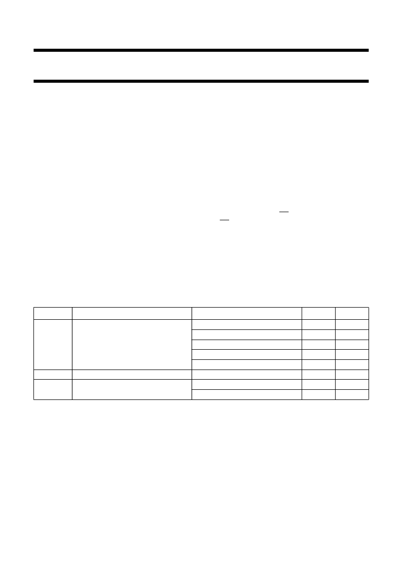
SYMBOL
PARAMETER
CONDITIONS
TYPICAL
UNIT
t
PHL
/t
PLH
propagation delay inputs nA to output nY V
CC
= 1.8 V; C
L
= 30 pF; R
L
= 1 k
4.5
2.8
2.8
2.6
2.1
2
20
5
ns
ns
ns
ns
ns
pF
pF
pF
V
CC
= 2.5 V; C
L
= 30 pF; R
L
= 500
V
CC
= 2.7 V; C
L
= 50 pF; R
L
= 500
V
CC
= 3.3 V; C
L
= 50 pF; R
L
= 500
V
CC
= 5.0 V; C
L
= 50 pF; R
L
= 500
C
I
C
PD
input capacitance
power dissipation capacitance per buffer
output enabled; notes 1 and 2
output disabled; notes 1 and 2
相關(guān)PDF資料 |
PDF描述 |
|---|---|
| 74LVC2G17GW | Dual non-inverting Schmitt-trigger with 5 V tolerant input |
| 74LVC2GU04 | Dual inverter |
| 74LVC2G240 | Dual buffer/line driver with 5 V tolerant inputs/outputs; inverting; 3-state |
| 74LVC2G32 | Dual 2-input OR gate |
| 74LVC2G66 | Bilateral switch |
相關(guān)代理商/技術(shù)參數(shù) |
參數(shù)描述 |
|---|---|
| 74LVC2G17GV,125 | 功能描述:緩沖器和線路驅(qū)動(dòng)器 3.3V DUAL SCHMITT TRIGG BUFF RoHS:否 制造商:Micrel 輸入線路數(shù)量:1 輸出線路數(shù)量:2 極性:Non-Inverting 電源電壓-最大:+/- 5.5 V 電源電壓-最小:+/- 2.37 V 最大工作溫度:+ 85 C 安裝風(fēng)格:SMD/SMT 封裝 / 箱體:MSOP-8 封裝:Reel |
| 74LVC2G17GV,125-CUT TAPE | 制造商:NXP 功能描述:74LVC Series 3.3 V Dual Non Inverting Schmitt Trigger - TSSOP-6 |
| 74LVC2G17GV-Q100H | 制造商:NXP Semiconductors 功能描述:74LVC2G17GV-Q100/SC-74/REELR// - Tape and Reel 制造商:NXP Semiconductors 功能描述:IC SCHMITT TRIGGER NON-INV 6TSOP |
| 74LVC2G17GW | 制造商:NXP Semiconductors 功能描述:Schmitt Trigger Buffer 2-CH Non-Inverting CMOS 6-Pin SOT-363 T/R |
| 74LVC2G17GW,125 | 功能描述:緩沖器和線路驅(qū)動(dòng)器 3.3V DUAL SCHMITT RoHS:否 制造商:Micrel 輸入線路數(shù)量:1 輸出線路數(shù)量:2 極性:Non-Inverting 電源電壓-最大:+/- 5.5 V 電源電壓-最小:+/- 2.37 V 最大工作溫度:+ 85 C 安裝風(fēng)格:SMD/SMT 封裝 / 箱體:MSOP-8 封裝:Reel |
發(fā)布緊急采購,3分鐘左右您將得到回復(fù)。