- 您現(xiàn)在的位置:買賣IC網(wǎng) > PDF目錄360423 > 74F109 (Fairchild Semiconductor Corporation) Dual JK Positive Edge-Triggered Flip-Flop PDF資料下載
參數(shù)資料
| 型號(hào): | 74F109 |
| 廠商: | Fairchild Semiconductor Corporation |
| 英文描述: | Dual JK Positive Edge-Triggered Flip-Flop |
| 中文描述: | 雙JK上升沿觸發(fā)器 |
| 文件頁(yè)數(shù): | 2/10頁(yè) |
| 文件大小: | 85K |
| 代理商: | 74F109 |
Philips Semiconductors
Product specification
74F109
Postive J-K positive edge-triggered flip-flops
2
October 23, 1990
853–0337 00783
FEATURE
Industrial temperature range available (–40
°
C to +85
°
C)
DESCRIPTION
The 74F109 is a dual positive edge-triggered JK-type flip-flop
featuring individual J, K, clock, set, and reset inputs; also true and
complementary outputs. Set (SD) and reset (RD) are asynchronous
active low inputs and operate independently of the clock (CP) input.
The J and K are edge-triggered inputs which control the state
changes of the flip-flops as described in the function table. Clock
triggering occurs at a voltage level and is not directly related to the
transition time of the positive-going pulse. The J and K inputs must
be stable just one setup time prior to the low-to-high transition of the
clock for predictable operation. The JK design allows operation as a
D flip-flop by tying J and K inputs together. Although the clock input
is level sensitive, the positive transition of the clock pulse between
the 0.8V and 2.0V levels should be equal to or less than the clock to
output delay time for reliable operation.
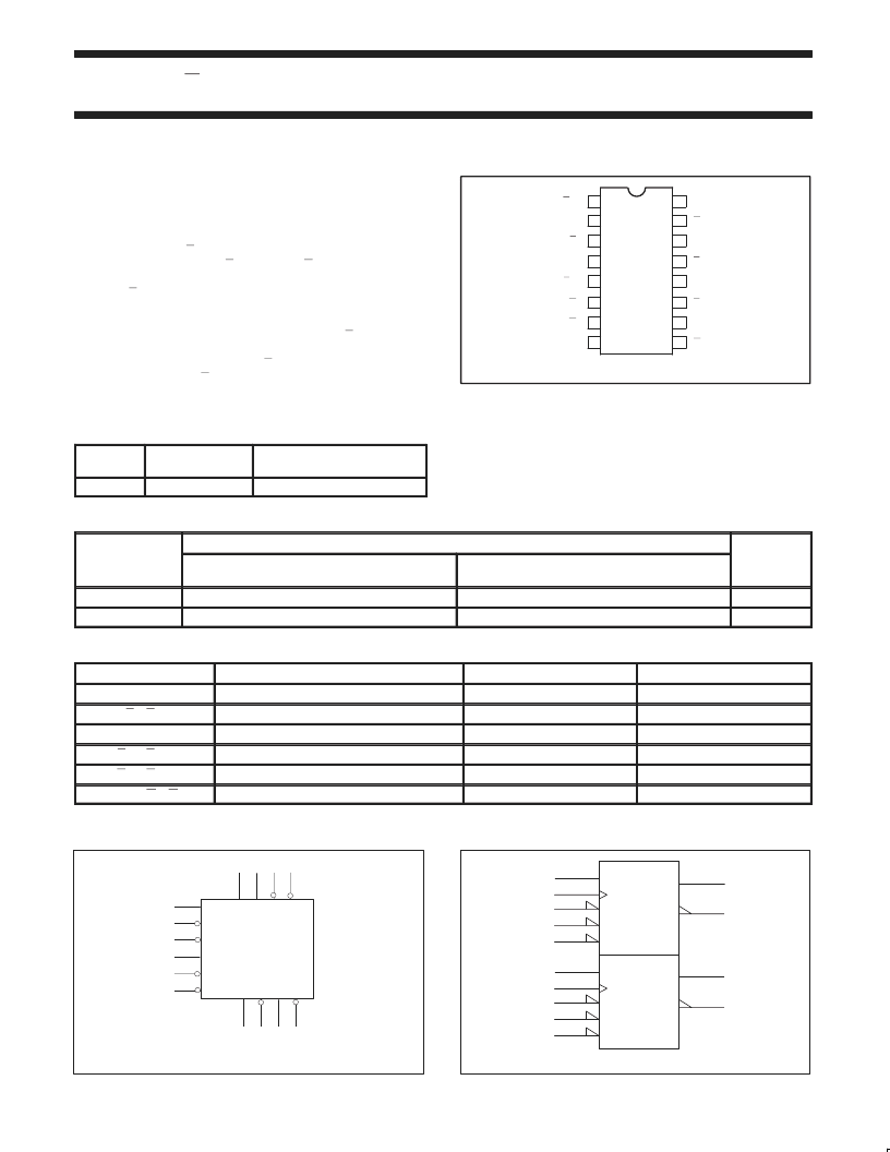
PIN CONFIGURATION
16
15
14
13
12
11
10
7
6
5
4
3
2
1
Q0
V
CC
CP1
SD1
Q1
K1
RD1
J1
RD0
J0
Q0
K0
CP0
SD0
9
8
GND
Q1
SF00135
TYPE
TYPICAL f
max
TYPICAL SUPPLY CURRENT
(TOTAL)
74F109
125MHz
12.3mA
ORDERING INFORMATION
ORDER CODE
DESCRIPTION
COMMERCIAL RANGE
V
CC
= 5V
±
10%, T
amb
= 0
°
C to +70
°
C
N74F109N
INDUSTRIAL RANGE
V
CC
= 5V
±
10%, T
amb
= –40
°
C to +85
°
C
I74F109N
PKG DWG #
16-pin plastic DIP
SOT38-4
16-pin plastic SO
N74F109D
I74F109D
SOT109-1
INPUT AND OUTPUT LOADING AND FAN OUT TABLE
PINS
DESCRIPTION
74F (U.L.) HIGH/LOW
LOAD VALUE HIGH/LOW
J0, J1
J inputs
1.0/1.0
20
μ
A/0.6mA
20
μ
A/0.6mA
20
μ
A/0.6mA
20
μ
A/1.8mA
20
μ
A/1.8mA
1.0mA/20mA
K0, K1
K inputs
1.0/1.0
CP0, CP1
Clock inputs (active rising edge)
1.0/1.0
SD0, SD1
Set inputs (active Low)
1.0/3.0
RD0, RD1
Reset inputs (active Low)
1.0/3.0
Q0, Q1, Q0, Q1
NOTE:
One (1.0) FAST unit load is defined as: 20
μ
A in the High state and 0.6mA in the Low state.
Data outputs
50/33
LOGIC SYMBOL
J1
J0
Q0 Q0 Q1 Q1
V
= Pin 16
GND = Pin 8
K1
K0
2 14 3 13
6 7 10 9
CP0
SD0
RD0
CP1
SD1
RD1
4
5
1
12
11
15
SF00136
IEC/IEEE SYMBOL
SF00137
7
2
4
3
1
5
14
12
13
15
11
6
10
9
1J
C1
1K
R
S
2J
C2
2K
R
S
相關(guān)PDF資料 |
PDF描述 |
|---|---|
| 74F109PC | Dual JK Positive Edge-Triggered Flip-Flop |
| 74F109SC | Dual JK Positive Edge-Triggered Flip-Flop |
| 74F109SJ | Dual JK Positive Edge-Triggered Flip-Flop |
| 74F112 | Dual J-K negative edge-triggered flip-flop |
| 74F112 | Dual JK Negative Edge-Triggered Flip-Flop |
相關(guān)代理商/技術(shù)參數(shù) |
參數(shù)描述 |
|---|---|
| 74F109_00 | 制造商:FAIRCHILD 制造商全稱:Fairchild Semiconductor 功能描述:Dual JK Positive Edge-Triggered Flip-Flop |
| 74F109_XGH3026B WAF | 制造商:Fairchild Semiconductor Corporation 功能描述: |
| 74F109D | 制造商:North American Philips Discrete Products Div 功能描述:Flip Flop, Dual, J/K Type, 16 Pin, Plastic, SOP 制造商:NXP Semiconductors 功能描述:Flip Flop, Dual, J/K Type, 16 Pin, Plastic, SOP |
| 74F109DC | 制造商:Rochester Electronics LLC 功能描述:- Bulk |
| 74F109LC | 制造商:Rochester Electronics LLC 功能描述:- Bulk |
發(fā)布緊急采購(gòu),3分鐘左右您將得到回復(fù)。