- 您現(xiàn)在的位置:買賣IC網(wǎng) > PDF目錄369228 > 66133-103 (MICROPAC INDUSTRIES INC) SINGLE CHANNEL OPTOCOUPLERS(REPLACEMENT FOR TIL 120) PDF資料下載
參數(shù)資料
| 型號: | 66133-103 |
| 廠商: | MICROPAC INDUSTRIES INC |
| 元件分類: | 光電耦合器 |
| 英文描述: | SINGLE CHANNEL OPTOCOUPLERS(REPLACEMENT FOR TIL 120) |
| 中文描述: | 1 CHANNEL TRANSISTOR OUTPUT OPTOCOUPLER |
| 封裝: | HERMETIC SEALED, TO-18, 4 PIN |
| 文件頁數(shù): | 1/2頁 |
| 文件大?。?/td> | 81K |
| 代理商: | 66133-103 |
MICROPAC INDUSTRIES, INC.
OPTOELECTRONIC PRODUCTS DIVISION
725 E. Walnut St., Garland, TX 75040
(972) 272-3571
Fax (972) 487-6918
www.micropac.com
E-MAIL: optosales@micropac.com
3 - 3
3N261
66133
3N262
SINGLE CHANNEL OPTOCOUPLERS
3N263
(REPLACEMENT FOR TIL 120)
Mii
OPTOELECTRONIC PRODUCTS
DIVISION
REVISION A 9/15/00
Features:
Electrically similar to 4N47, 4N48, 4N49
Base lead eliminated for improved noise immunity
Rugged package
+1kV electrical isolation
Stability over wide temperature range
Applications:
Eliminate ground loops
Level shifting
Line receiver
Switching power supplies
Motor control
DESCRIPTION
The
66133
single channel optocoupler consists of a Gallium Arsenide infrared LED and a high gain N-P-N silicon
phototransistor packaged in a hermetically sealed metal case. The
3N261
,
3N262
and
3N263
’s can be tested to customer
specifications, as well as to MIL-PRF-19500 using Micropac’s extensive in-house test facilities.
ABSOLUTE MAXIMUM RATINGS
Input to Output Voltage.............................................................................................................................................................1kV
Emitter-Collector Voltage............................................................................................................................................................7V
Collector-Emitter Voltage (
V
CEO
,
I
F
=
0
).....................................................................................................................................40V
Reverse Input Voltage ...............................................................................................................................................................2V
Input Diode Continuous Forward Current at (or below) 65°C Free-Air Temperature (see note 1)......................................40mA
Peak Forward Input Current (Value applies for tw
<
1
μ
s, PRR
<
300 pps) ...............................................................................1A
Continuous Collector Current................................................................................................................................................20mA
Continuous Transistor Power Dissipation at (or below) 25°C Free-Air Temperature (see Note 2) .................................275mW
Storage Temperature........................................................................................................................................... -65°C to +150°C
Operating Free-Air Temperature Range............................................................................................................. -55°C to +100°C
Lead Solder Temperature (10 seconds max.) .....................................................................................................................240°C
Notes:
1. Derate linearly to 100°C free-air temperature at the rate of 1.14 mA/
°
C above 65°C.
2. Derate linearly to 100°C free-air temperature at the rate of 7.8 mW/
°
C above 65°C.
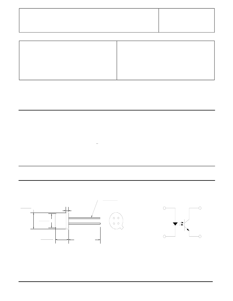
Package Dimensions Schematic Diagram
0.500 [12.70]
MIN
4 LEADS
GOLD PLATED KOVAR
0.019 [0.48]
0.016 [0.41]
0.210 [5.33]
170 [4.32]
0.040 [1.02]MAX
.195 [4.95]
.178 [4.52]
.230 [5.84]
.209 [5.31]
1
4
3
2
NOTE 1: THIS DIMENSION IS CONTROLLED AT THE HOUSING SURFACE.
DIMENSIONS ARE IN INCHES [MILLIMETERS]
SEE NOTE 1
1.00 [2.54]
2
4
1
3
BOTTOM VIEW
THE COLLECTOR IS IN ELECTRICAL CONTACT WITH THE CASE
相關(guān)PDF資料 |
PDF描述 |
|---|---|
| 66133 | SINGLE CHANNEL OPTOCOUPLERS(REPLACEMENT FOR TIL 120) |
| 66147-001 | 40kV HIGH VOLTAGE ISOLATOR WITH BUFFERED OUTPUT |
| 66147-011 | AC-DC Power Supply Cover Kit; ; Category: AC-DC; Type: Low to Medium; Length: 5.9; Width: 3.86; Height: 1.97 |
| 66147-102 | 40kV HIGH VOLTAGE ISOLATOR WITH BUFFERED OUTPUT |
| 66147 | 40kV HIGH VOLTAGE ISOLATOR WITH BUFFERED OUTPUT |
相關(guān)代理商/技術(shù)參數(shù) |
參數(shù)描述 |
|---|---|
| 66-13332MA-00 | 制造商: 功能描述: 制造商:undefined 功能描述: |
| 661-33AB | 制造商:WAKEFIELD-VETTE 功能描述:BOARD LEVEL HEAT SINK 制造商:WAKEFIELD THERMAL SOLUTIONS 功能描述:Heat Sink Passive Black Anodized |
| 661-33ABT1 | 制造商:WAKEFIELD THERMAL SOLUTIONS 功能描述:BGA Htsink |
| 66133ABT111476969 | 制造商:WAK 功能描述:WAKEFIELD S7D8B-NOTES |
| 661-33ABT2 | 制造商:WAKEFIELD THERMAL SOLUTIONS 功能描述:BGA Htsink |
發(fā)布緊急采購,3分鐘左右您將得到回復(fù)。