- 您現(xiàn)在的位置:買賣IC網(wǎng) > PDF目錄369228 > 66147-011 (MICROPAC INDUSTRIES INC) AC-DC Power Supply Cover Kit; ; Category: AC-DC; Type: Low to Medium; Length: 5.9; Width: 3.86; Height: 1.97 PDF資料下載
參數(shù)資料
| 型號(hào): | 66147-011 |
| 廠商: | MICROPAC INDUSTRIES INC |
| 元件分類: | 光電耦合器 |
| 英文描述: | AC-DC Power Supply Cover Kit; ; Category: AC-DC; Type: Low to Medium; Length: 5.9; Width: 3.86; Height: 1.97 |
| 中文描述: | 1 CHANNEL LOGIC OUTPUT OPTOCOUPLER |
| 封裝: | HERMETIC SEALED, CERAMIC, TO-46, 5 PIN |
| 文件頁(yè)數(shù): | 1/2頁(yè) |
| 文件大?。?/td> | 91K |
| 代理商: | 66147-011 |
MICROPAC INDUSTRIES, INC.
OPTOELECTRONIC PRODUCTS DIVISION
725 E. Walnut St., Garland, TX 75040
(972) 272-3571
Fax (972) 487-6918
www.micropac.com
E-MAIL:
optosales@micropac.com
7 - 7
66147
40kV HIGH VOLTAGE ISOLATOR WITH BUFFERED OUTPUT
Mii
OPTOELECTRONIC PRODUCTS
DIVISION
Features:
10 Mhz bandwidth typical
40kVdc isolation test voltage
TTL compatible input and output
High common mode rejection
Rugged ceramic package
Applications:
Military and Space
Voltage Level Shifting
Grid Current Modulator
Switching between power supplies
Medical systems
DESCRIPTION
The
66147
high voltage isolation consisting of a LED optically coupled to a high speed, high gain inverting detector gate.
Output is TTL capable with switching propagation delays of 55ns typical, hermetically sealed in TO-46 packages and mounted
in a highly reliability, hermetically sealed ceramic package. Available in commercial (0
°
to +70
°
C), extended temperature range
(-40
°
to +85
°
) and full Military temperature range (-55
°
to +125
°
C).
Contact the factory for special custom or multi-channel
requirements!
ABSOLUTE MAXIMUM RATINGS
Storage Temperature........................................................................................................................................... -65
°
C to +150
°
C
Operating Free-Air Temperature Range............................................................................................................. -55
°
C to +125
°
C
Lead Solder Temperature.........................................................................................260
°
C for 10s (1.6mm below seating plane)
Peak Forward Input Current ........................................................................................................................40mA (1ms duration)
Average Forward Input Current ............................................................................................................................................20mA
Input Power Dissipation .......................................................................................................................................................35mW
Reverse Input Voltage ...............................................................................................................................................................5V
Supply voltage - V
CC
................................................................................................................................. 7V(1 minute maximum)
Output Current - I
O
................................................................................................................................................................25mA
Output Power Dissipation ....................................................................................................................................................40mW
Output Voltage - V
O
...................................................................................................................................................................7V
Total Power Dissipation .....................................................................................................................................................350mW
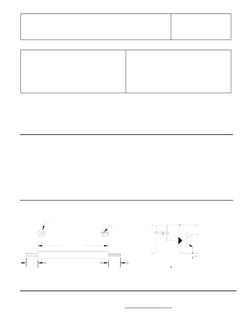
Package Dimensions
Schematic Diagram
Vcc AND GROUND.
CONNECTED BETWEEN
CAPACITOR MUST BE
A.01 TO 0.1
NOTE:
F BYPASS
GND
CASE
Vout
VCC
A
K
3.000 [76.20]
K
Vcc
GND(RED DOT)
CASE
Vout
A (BLACK DOT)
0.300 [7.62]
0.500 [12.70]
MIN
0.500 [12.70]
0.018 [0.46]
TYP
DIMENSIONS ARE INCHES(MILLIMETERS) NOMINAL
相關(guān)PDF資料 |
PDF描述 |
|---|---|
| 66147-102 | 40kV HIGH VOLTAGE ISOLATOR WITH BUFFERED OUTPUT |
| 66147 | 40kV HIGH VOLTAGE ISOLATOR WITH BUFFERED OUTPUT |
| 66153-101 | SILICON PHOTOTRANSISTOR “PIGTAIL” |
| 66155-101 | SILICON PHOTOTRANSISTOR “PILL PACK” |
| 66156 | SINGLE CHANNEL OPTOCOUPLER PHOTODIODE OUTPUT COAXIAL OR BULKHEAD MOUNT PACKAGES |
相關(guān)代理商/技術(shù)參數(shù) |
參數(shù)描述 |
|---|---|
| 66147-102 | 制造商:MII 制造商全稱:MII 功能描述:40kV HIGH VOLTAGE ISOLATOR WITH BUFFERED OUTPUT |
| 66147-108 | 制造商:FCI 功能描述:DISCONTINUED SERIES,NO REPL |
| 66148 | 制造商:未知廠家 制造商全稱:未知廠家 功能描述:SPRAY GEGEN SCHEWEISSSPRITZTEN 400ML |
| 661496-000 | 制造商:TE Connectivity 功能描述:- Bulk |
| 6614A30001D | 制造商:LG Corporation 功能描述:Controller Assembly |
發(fā)布緊急采購(gòu),3分鐘左右您將得到回復(fù)。