- 您現(xiàn)在的位置:買賣IC網(wǎng) > PDF目錄97783 > 5962-9086102Q2A (TEXAS INSTRUMENTS INC) DUAL OP-AMP, 6500 uV OFFSET-MAX, 1 MHz BAND WIDTH, CQCC20 PDF資料下載
參數(shù)資料
| 型號: | 5962-9086102Q2A |
| 廠商: | TEXAS INSTRUMENTS INC |
| 元件分類: | 運算放大器 |
| 英文描述: | DUAL OP-AMP, 6500 uV OFFSET-MAX, 1 MHz BAND WIDTH, CQCC20 |
| 封裝: | CERAMIC, LCC-20 |
| 文件頁數(shù): | 56/71頁 |
| 文件大小: | 1577K |
| 代理商: | 5962-9086102Q2A |
第1頁第2頁第3頁第4頁第5頁第6頁第7頁第8頁第9頁第10頁第11頁第12頁第13頁第14頁第15頁第16頁第17頁第18頁第19頁第20頁第21頁第22頁第23頁第24頁第25頁第26頁第27頁第28頁第29頁第30頁第31頁第32頁第33頁第34頁第35頁第36頁第37頁第38頁第39頁第40頁第41頁第42頁第43頁第44頁第45頁第46頁第47頁第48頁第49頁第50頁第51頁第52頁第53頁第54頁第55頁當前第56頁第57頁第58頁第59頁第60頁第61頁第62頁第63頁第64頁第65頁第66頁第67頁第68頁第69頁第70頁第71頁
TL03x, TL03xA
ENHANCED-JFET LOW-POWER LOW-OFFSET
OPERATIONAL AMPLIFIERS
SLOS180C FEBRUARY 1997 REVISED DECEMBER 2001
6
POST OFFICE BOX 655303
DALLAS, TEXAS 75265
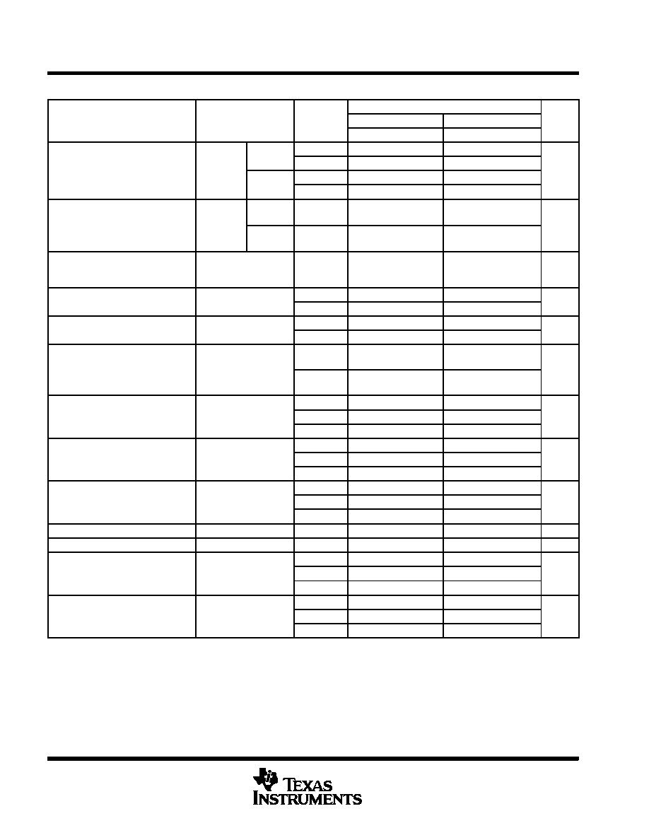
TL031C and TL031AC electrical characteristics at specified free-air temperature
TL031C, TL031AC
PARAMETER
TEST CONDITIONS
TA
VCC± = ±5 V
VCC± = ±15 V
UNIT
PARAMETER
TEST CONDITIONS
TA
MIN
TYP
MAX
MIN
TYP
MAX
UNIT
TL031C
25
°C
0.54
3.5
0.5
1.5
V
Input offset voltage
VO = 0,
V
0
TL031C
Full range
4.5
2.5
mV
VIO
Input offset voltage
VIC = 0,
RS = 50 Ω
TL031AC
25
°C
0.41
2.8
0.34
0.8
mV
RS = 50 Ω
TL031AC
Full range
3.8
1.8
TL031C
25
°C to
71
59
a
Temperature coefficient of
VO = 0,
V
0
TL031C
25 C to
70
°C
7.1
5.9
V/
°C
a
V
IO
Temperature coefficient of
input offset voltage
VIC =0,
RS = 50 Ω
TL031AC
25
°C to
71
59
25
μV/°C
input offset voltage
RS = 50 Ω
TL031AC
25 C to
70
°C
7.1
5.9
25
Input offset voltage
long-term drift
VO = 0,
VIC =0,
RS = 50 Ω
25
°C
0.04
μV/mo
I
Input offset current
VO = 0, VIC = 0
25
°C
1
100
1
100
pA
IIO
Input offset current
VO = 0, VIC = 0
See Figure 5
70
°C
9
200
12
200
pA
I
Input bias current
VO = 0, VIC = 0
25
°C
2
200
2
200
pA
IIB
Input bias current
VO = 0, VIC = 0
See Figure 5
70
°C
50
400
80
400
pA
V
Common-mode input
25
°C
1.5
to 4
3.4
to 5.4
11.5
to 14
13.4
to 15.4
V
VICR
Common mode input
voltage range
Full range
1.5
to 4
11.5
to 14
V
M
i
iti
k
25
°C
3
4.3
13
14
VOM+
Maximum positive peak
output voltage swing
RL = 10 kΩ
0
°C
3
4.2
13
14
V
VOM+
output voltage swing
RL
10 k
Ω
70
°C
3
4.3
13
14
V
Mi
ti
k
25
°C
3
4.2
12.5
13.9
VOM
Maximum negative peak
output voltage swing
RL = 10 kΩ
0
°C
3
4.1
12.5
13.9
V
VOM
output voltage swing
RL
10 k
Ω
70
°C
3
4.2
12.5
14
V
25
°C
4
12
5
14.3
AVD
Large-signal differential
voltage amplification§
RL = 10 kΩ
0
°C
3
11.1
4
13.5
V/mV
AVD
voltage amplification§
RL
10 k
Ω
70
°C
4
13.3
5
15.2
V/mV
ri
Input resistance
25
°C
1012
Ω
ci
Input capacitance
25
°C
5
4
pF
Cd
V
i
25
°C
70
87
75
94
CMRR
Common-mode
rejection ratio
VIC = VICRmin,
VO =0 RS =50 Ω
0
°C
70
87
75
94
dB
CMRR
rejection ratio
VO = 0, RS = 50 Ω
70
°C
70
87
75
94
dB
Supply-voltage
25
°C
75
96
75
96
kSVR
Supply-voltage
rejection ratio
VO = 0, RS = 50 Ω
0
°C
75
96
75
96
dB
SVR
rejection ratio
(
ΔVCC±/ΔVIO)
O
,
S
70
°C
75
96
75
96
Full range is 0
°C to 70°C.
Typical values are based on the input offset voltage shift observed through 168 hours of operating life test at TA = 150°C extrapolated to
TA = 25°C using the Arrhenius equation and assuming an activation energy of 0.96 eV.
§ At VCC± = ±5 V, VO = ±2.3 V; at VCC± = ±15 V, VO = ±10 V
相關PDF資料 |
PDF描述 |
|---|---|
| 5962-9088101M2A | OP-AMP, 500 uV OFFSET-MAX, 2 MHz BAND WIDTH, CQCC20 |
| 5962-9088105QPX | DUAL OP-AMP, 450 uV OFFSET-MAX, 2.8 MHz BAND WIDTH, CDIP8 |
| 5962-9088203V2A | OP-AMP, 400 uV OFFSET-MAX, 1.8 MHz BAND WIDTH, CQCC20 |
| 5962-9089501MCA | OP-AMP, 8 uV OFFSET-MAX, 1.9 MHz BAND WIDTH, CDIP14 |
| 5962-9089501MPA | OP-AMP, 10 uV OFFSET-MAX, 1.9 MHz BAND WIDTH, CDIP8 |
相關代理商/技術參數(shù) |
參數(shù)描述 |
|---|---|
| 5962-9086403MXC | 制造商:Atmel Corporation 功能描述: |
| 5962-9086801MXC | 制造商:Rochester Electronics LLC 功能描述:- Bulk |
| 5962-9086802MXX | 制造商:Analog Devices 功能描述:- Rail/Tube |
| 5962-9086803MXC | 制造商:Rochester Electronics LLC 功能描述:- Bulk |
| 5962-9086804MXC | 制造商:Rochester Electronics LLC 功能描述:- Bulk |
發(fā)布緊急采購,3分鐘左右您將得到回復。