- 您現(xiàn)在的位置:買賣IC網(wǎng) > PDF目錄97781 > 5962-88721012A (ANALOG DEVICES INC) DUAL OP-AMP, 175 uV OFFSET-MAX, 5 MHz BAND WIDTH, CQCC20 PDF資料下載
參數(shù)資料
| 型號(hào): | 5962-88721012A |
| 廠商: | ANALOG DEVICES INC |
| 元件分類: | 運(yùn)算放大器 |
| 英文描述: | DUAL OP-AMP, 175 uV OFFSET-MAX, 5 MHz BAND WIDTH, CQCC20 |
| 封裝: | CERAMIC, LCC-20 |
| 文件頁(yè)數(shù): | 4/16頁(yè) |
| 文件大小: | 1708K |
| 代理商: | 5962-88721012A |
第1頁(yè)第2頁(yè)第3頁(yè)當(dāng)前第4頁(yè)第5頁(yè)第6頁(yè)第7頁(yè)第8頁(yè)第9頁(yè)第10頁(yè)第11頁(yè)第12頁(yè)第13頁(yè)第14頁(yè)第15頁(yè)第16頁(yè)

REV. B
OP270
–12–
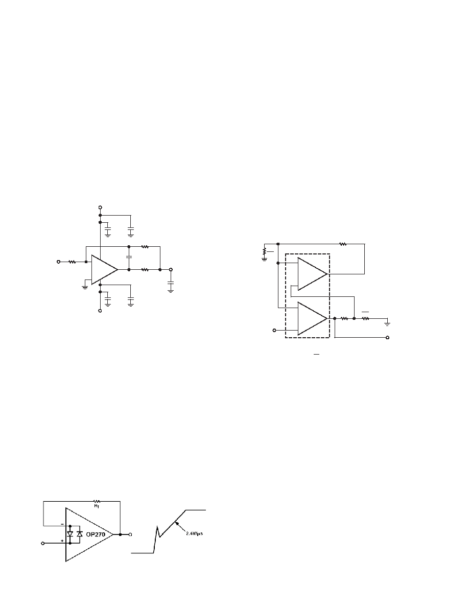
CAPACITIVE LOAD DRIVING AND POWER SUPPLY
CONSIDERATIONS
The OP270 is unity-gain stable and is capable of driving large
capacitive loads without oscillating. Nonetheless, good supply
bypassing is highly recommended. Proper supply bypassing
reduces problems caused by supply line noise and improves the
capacitive load driving capability of the OP270.
In the standard feedback amplifier, the op amp’s output resis-
tance combines with the load capacitance to form a lowpass
filter that adds phase shift in the feedback network and reduces
stability. A simple circuit to eliminate this effect is shown in
Figure 10. The added components, C1 and R3, decouple the
amplifier from the load capacitance and provide additional
stability. The values of C1 and R3 shown in Figure 10 are for a
load capacitance of up to 1000 pF when used with the OP270.
OP270
–
+
R1
VIN
R3
50
C1
200pF
R2
VOUT
C1
1000pF
PLACE SUPPLY DECOUPLING
CAPACITOR AT OP270
C5
0.1 F
C4
10 F
+
V–
C3
0.1 F
C2
10 F
+
V+
Figure 10. Driving Large Capacitive Loads
UNITY-GAIN BUFFER APPLICATIONS
When Rf
100W and the input is driven with a fast, large signal
pulse (>1 V), the output waveform will look as shown in Figure 11.
During the fast feedthrough-like portion of the output, the input
protection diodes effectively short the output to the input, and a
current, limited only by the output short-circuit protection, will be
drawn by the signal generator. With Rf
≥ 500 W, the output is
capable of handling the current requirements (IL
20 mA at 10 V);
the amplifier will stay in its active mode and a smooth transition
will occur.
When Rf > 3 k
W, a pole created by Rf and the amplifier’s input
capacitance (3 pF) creates additional phase shift and reduces
phase margin. A small capacitor (20 pF to 50 pF) in parallel
with Rf helps eliminate this problem.
Figure 11. Pulsed Operation
APPLICATIONS
LOW PHASE ERROR AMPLIFIER
The simple amplifier depicted in Figure 12 utilizes a monolithic
dual operational amplifier and a few resistors to substantially
reduce phase error compared to conventional amplifier designs.
At a given gain, the frequency range for a specified phase accuracy is
over a decade greater than for a standard single op amp amplifier.
The low phase error amplifier performs second-order fre-
quency compensation through the response of op amp A2 in
the feedback loop of A1. Both op amps must be extremely
well matched in frequency response. At low frequencies, the
A1 feedback loop forces V2 /(K1 + 1) = VIN. The A2 feedback
loop forces Vo/(K1 + 1) = V2 /(K1 + 1) yielding an overall
transfer function of VO/VIN = K1 + 1. The DC gain is deter-
mined by the resistor divider at the output, VO, and is not
directly affected by the resistor divider around A2. Note, that
like a conventional single op amp amplifier, the DC gain is set
by resistor ratios only. Minimum gain for the low phase error
amplifier is 10.
1/2
OP270E
A2
–
+
1/2
OP270E
A1
–
+
R2
K1
R2
R2 = R1
V2
R2
R1
K1
VO
VO = (K1 + 1) VIN
ASSUME: A1 AND A1 ARE MATCHED.
AO(s) =
T
s
VIN
Figure 12. Low Phase Error Amplifier
Figure 12 compares the phase error performance of the low
phase error amplifier with a conventional single op amp ampli-
fier and a cascaded two-stage amplifier. The low phase error
amplifier shows a much lower phase error, particularly for fre-
quencies where
w/bwT < 0.1. For example, phase error of -0.1∞
occurs at 0.002
w/bwT for the single op amp amplifier, but at
0.11
w/bwT for the low phase error amplifier.
For more detailed information on the low phase error amplifier,
see Application Note AN-107.
相關(guān)PDF資料 |
PDF描述 |
|---|---|
| 5962-8872101PA | DUAL OP-AMP, 175 uV OFFSET-MAX, 5 MHz BAND WIDTH, CDIP8 |
| 5962-8949403PA | DUAL OP-AMP, 12000 uV OFFSET-MAX, 0.085 MHz BAND WIDTH, CDIP8 |
| 5962-89494032A | DUAL OP-AMP, 12000 uV OFFSET-MAX, 0.085 MHz BAND WIDTH, CQCC20 |
| 5962-89494042A | DUAL OP-AMP, 3750 uV OFFSET-MAX, 0.14 MHz BAND WIDTH, CQCC20 |
| 5962-8949404PA | DUAL OP-AMP, 3750 uV OFFSET-MAX, 0.14 MHz BAND WIDTH, CDIP8 |
相關(guān)代理商/技術(shù)參數(shù) |
參數(shù)描述 |
|---|---|
| 59628872101PA | 制造商:AD 功能描述:OP270-009Z |
| 5962-8872101PA | 制造商:Analog Devices 功能描述:OP Amp Dual GP 制造商:Analog Devices 功能描述:OP AMP DUAL GP 18V 8CDIP - Rail/Tube 制造商:Analog Devices 功能描述:DUAL PRECISION INSTR. AMPLIFIER ((NS)) 制造商:Analog Devices Inc. 功能描述:DUAL LOW-NOISE IC 制造商:Analog Devices Inc. 功能描述:Precision Amplifiers DUAL LOW-NOISE IC |
| 5962-8872101V2A | 制造商:Analog Devices 功能描述:DUAL,LOW-NOISE IC - Rail/Tube |
| 5962-8872101VPA | 制造商:Analog Devices 功能描述:HIGH-PERFORMANCE MONOLITHIC DUAL OP AMP OP270AZ/QMLV - Rail/Tube |
| 5962-88721022A | 制造商:Rochester Electronics LLC 功能描述:DUAL, HI-SPEED IC - Bulk |
發(fā)布緊急采購(gòu),3分鐘左右您將得到回復(fù)。