- 您現(xiàn)在的位置:買賣IC網(wǎng) > PDF目錄360230 > 508669A IC SMD PDF資料下載
參數(shù)資料
| 型號(hào): | 508669A |
| 英文描述: | IC SMD |
| 中文描述: | 集成電路貼片 |
| 文件頁(yè)數(shù): | 5/12頁(yè) |
| 文件大小: | 285K |
| 代理商: | 508669A |
5
LT1180A/LT1181A
C
HARA TERISTICS
U
A
TYPICAL PERFOR
CE
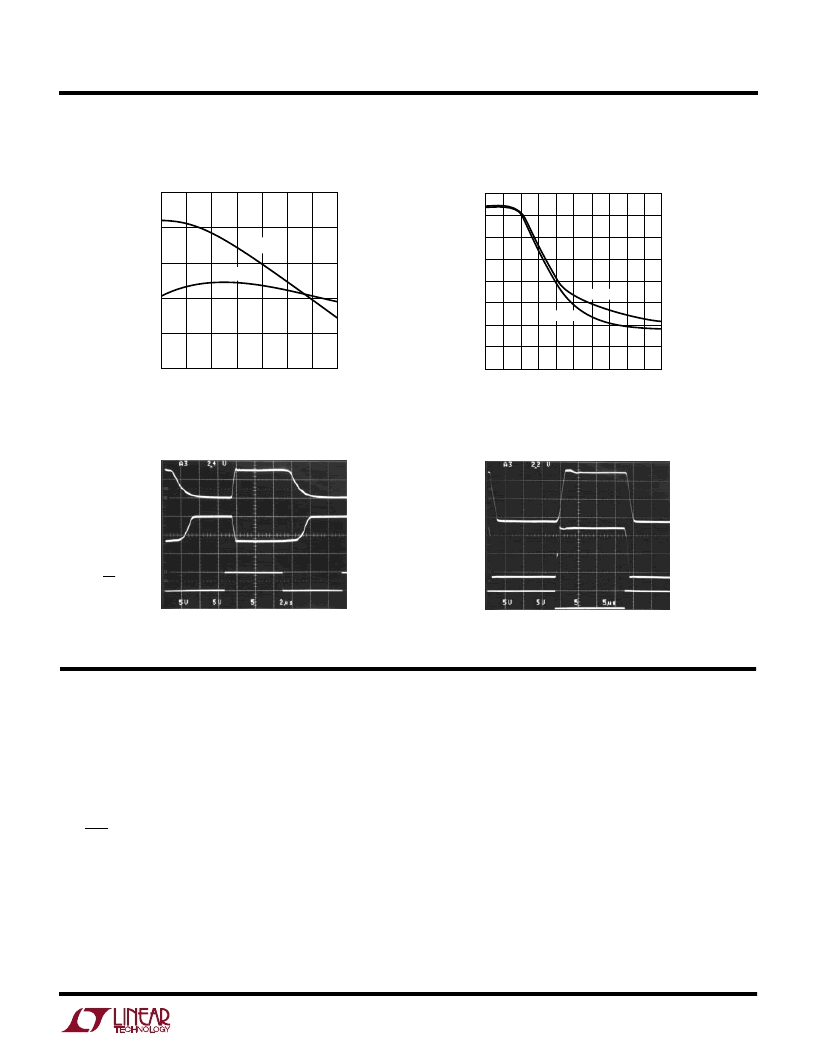
LOAD CAPACITANCE (nF)
0
S
12
16
4.0
LT1180A TPC11
8
4
0
1.0
2.0
3.0
5.0
10
14
6
2
3.5
0.5
1.5
2.5
4.5
+SLEW
–SLEW
LT1180A TPC13
LT1180A TPC12
INPUT
DRIVER OUTPUT
R
L
= 3k
DRIVER OUTPUT
R
= 3k
C
L
= 2500pF
DRIVER 1
OUTPUT
ON/OFF PIN
Shutdown to Driver Outputs
Driver Output Waveforms
10V
5V
GND
GND
–10V
–5V
DRIVER 2
OUTPUT
Slew Rate vs Load Capacitance
Receiver Short-Circuit Current
PI FU
V
CC
:
5V Input Supply Pin. This pin should be decoupled
with a 0.1
μ
F ceramic capacitor close to the package pin.
Insufficient supply bypassing can result in low output
drive levels and erratic charge pump operation.
GND:
Ground Pin.
ON/OFF:
A TTL/CMOS Compatible Operating Mode Con-
trol. A logic low puts the LT1180A in shutdown mode.
Supply current drops to zero and both driver and receiver
outputs assume a high impedance state. A logic high fully
enables the device.
U
V
+
:
Positive Supply Output (RS232 Drivers). V
+
≈
2V
CC
–
1.5V. This pin requires an external charge storage capaci-
tor C
≥
0.1
μ
F, tied to ground or V
CC
. Larger value capaci-
tors may be used to reduce supply ripple. With multiple
transceivers, the V
+
and V
–
pins may be paralleled into
common capacitors.
V
–
:
Negative Supply Output (RS232 Drivers). V
–
≈
–(2V
CC
– 2.5V). This pin requires an external charge storage
capacitor C
≥
0.1
μ
F. Larger value capacitors may be used
to reduce supply ripple. With multiple transceivers, the V
+
and V
–
pins may be paralleled into common capacitors.
TEMPERATURE (
°
C)
–55
0
S
20
50
0
50
75
LT1180A TPC10
10
40
30
–25
25
100
125
RX I
SC–
RX I
SC+
相關(guān)PDF資料 |
PDF描述 |
|---|---|
| 514409G | Dual/Triple Ultra-Low-Voltage SOT23 µP Supervisory Circuits |
| 522923D | Dual/Triple Ultra-Low-Voltage SOT23 µP Supervisory Circuits |
| 522929C | IC |
| 522946A | Dual/Triple Ultra-Low-Voltage SOT23 µP Supervisory Circuits |
| 522925X | IC |
相關(guān)代理商/技術(shù)參數(shù) |
參數(shù)描述 |
|---|---|
| 5086C10 | 制造商:Cinch Connectors 功能描述: |
| 5086-H-ABC0-D-E | 制造商:SCHURTER 制造商全稱:Schurter Inc. 功能描述:IEC Appliance Outlet D, insert Mounting, Solder Terminal |
| 5086-J1R | 制造商:GC Electronics 功能描述: |
| 5086X1100A5 | 制造商:Schurter Electronic Components 功能描述: |
| 5087 | 制造商:ELECTRONIC INDUSTRIES ASS 功能描述: |
發(fā)布緊急采購(gòu),3分鐘左右您將得到回復(fù)。